Best Semicon Manufacturing Suppliers
Discover a curated list of global semiconductor manufacturing partners offering advanced fabrication processes, cutting-edge technology, and customization options for diverse electronic applications.
SemiconductorsManufacturingFabricationMicroelectronicsChip Design
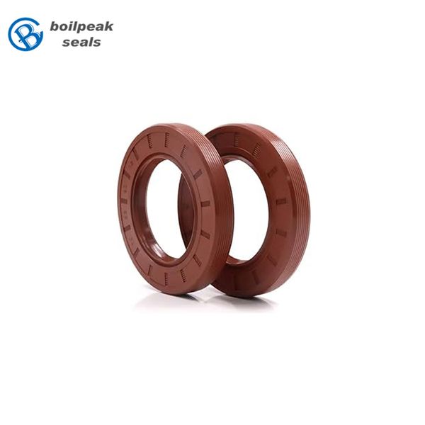
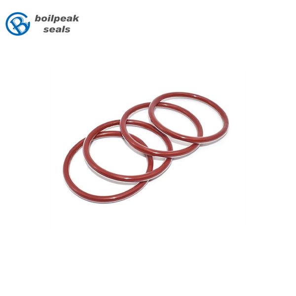
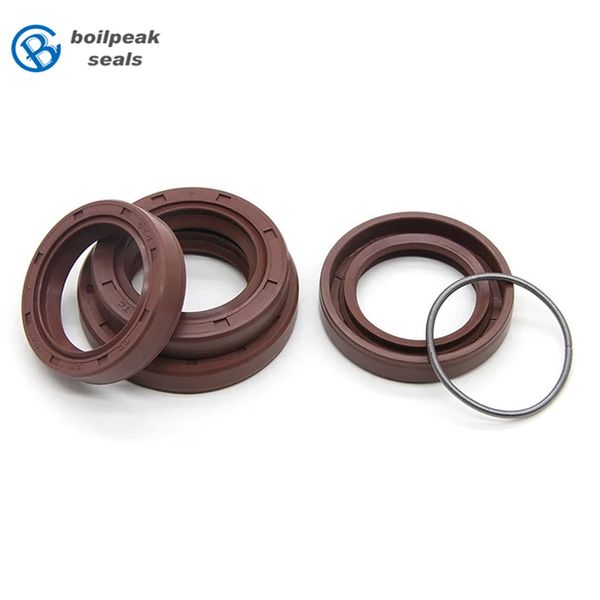
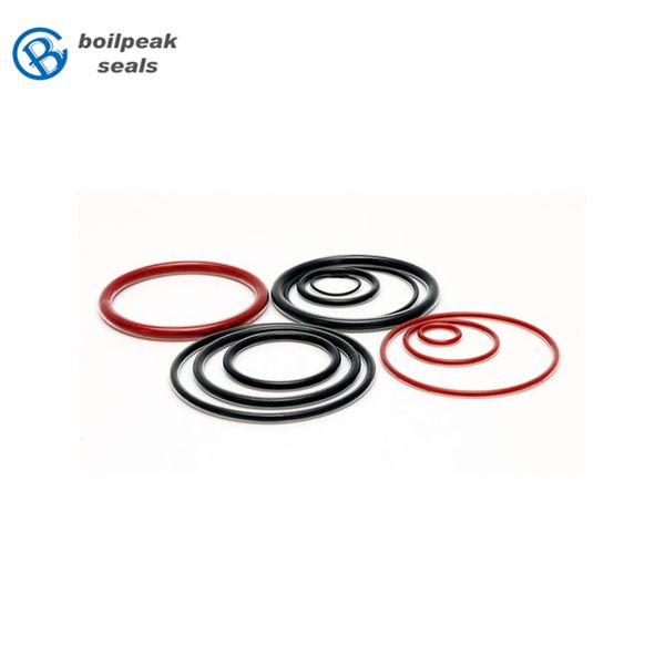
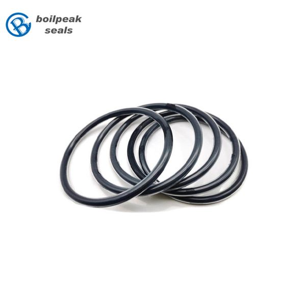
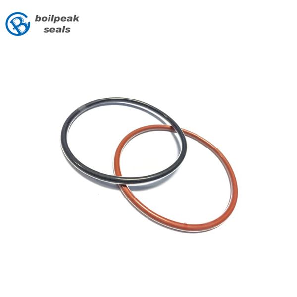
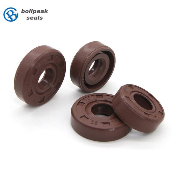
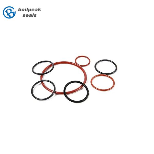
Shenzhen Boilpeak Seals Technology Co., Ltd.
🇨🇳 China
2014201-300 peopleManufacturer/Trading CompanyProduct customization
High-tech enterprise
Small batch production
Patented technology
Key customer
ALPHA
Key market
Europe
Description
Shenzhen Boilpeak Seals Technology Co., Ltd. is a professional manufacturer and integrated trading company established in 2014, specializing in the research, development, and production of high-performance sealing solutions. Based in Huai'an, Jiangsu, the company operates a 20,000-square-meter facility that includes a dedicated Technology Center and 4,500 square meters of cleanroom environments (Class 100 and Class 1000). With a workforce of 201 to 300 employees and annual revenue exceeding US$100 million, the company is a trusted partner for global industries requiring precision-engineered components.
Wholesale High Quality TC NBR and FKM Oil Seals Rubber Oil Seal Manufactured in China$1.2
High Quality High-Pressure FEP (PFA) Encapsulated FKM Silicone O-Ring Seal Premium Seals Material$0.01
TC/TG Series Complete Set of Nitrile/FKM Oil Seals Full Specifications for Abrasion-Resistant Oil-Resistant Seals$1.2

PTFE Encapsulated FKM Silicone O-Ring Seals Product Category$0.01
FKM VMQ High Temperature Industrial Circle O-Ring Seal Rubber Encapsulated Seals for Extreme Conditions$0.01
OEM High Temperature Resistanc PTFE Encapsulated FKM Silicone Rubber O-Ring Seals Product$0.01
Encapsulated O-Ring Seal with Inner FKM VMQ Rubber PFA FEP Product Category Seals$0.01

PTFE Encapsulated PFA FEP O-Ring Coating FKM FPM Rubber with VMQ Silicone Inner Hollow Seals Product$0.01
High Quality Corrosion and Wear Resistant High Temperature TC Skeleton Oil Seals NBR and FKM Materials$1.2

Factory Price FKM Silicone O-Ring FEP/PFA Encapsulated Seal Ring Premium Seals$0.01
High-Temperature Resistance PTFE Encapsulated O-Ring PFA FEP O-RING Coating with FKM VMQ Rubber for Inner Seals$0.01
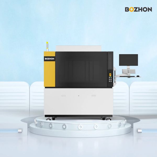
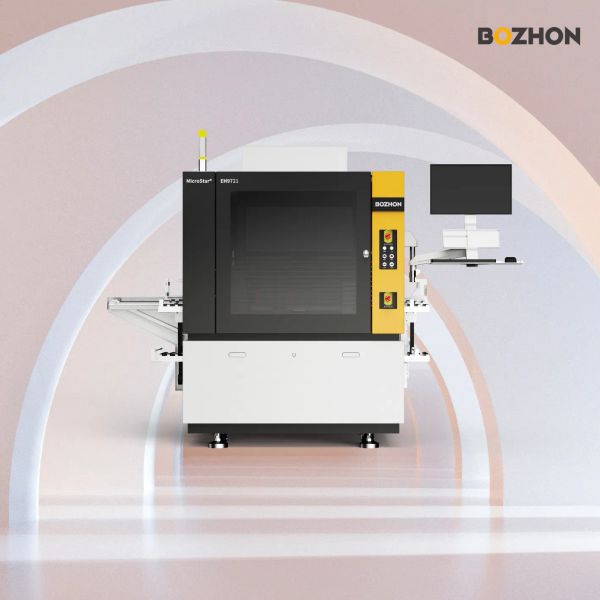
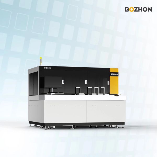
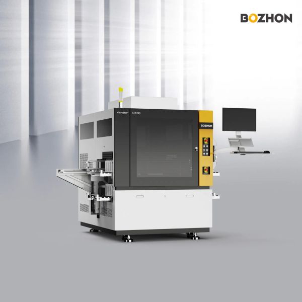
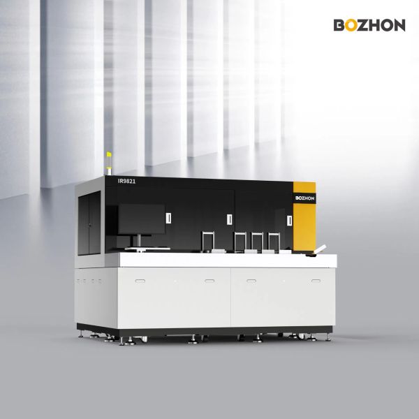
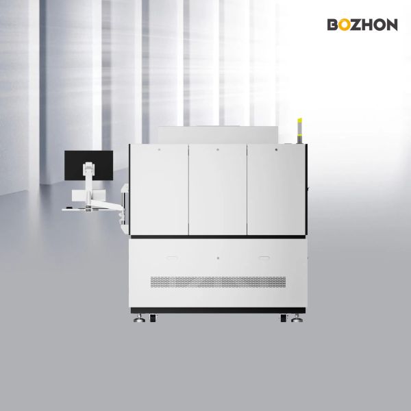
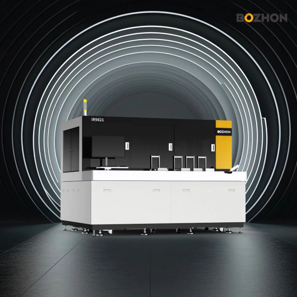
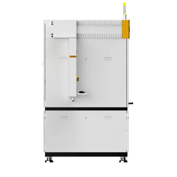
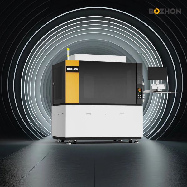
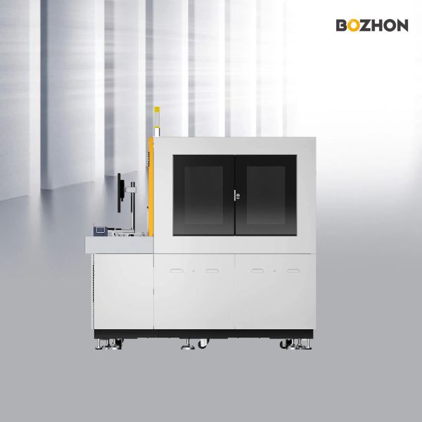
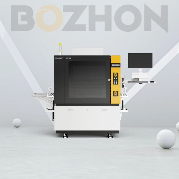
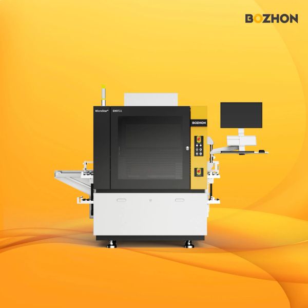
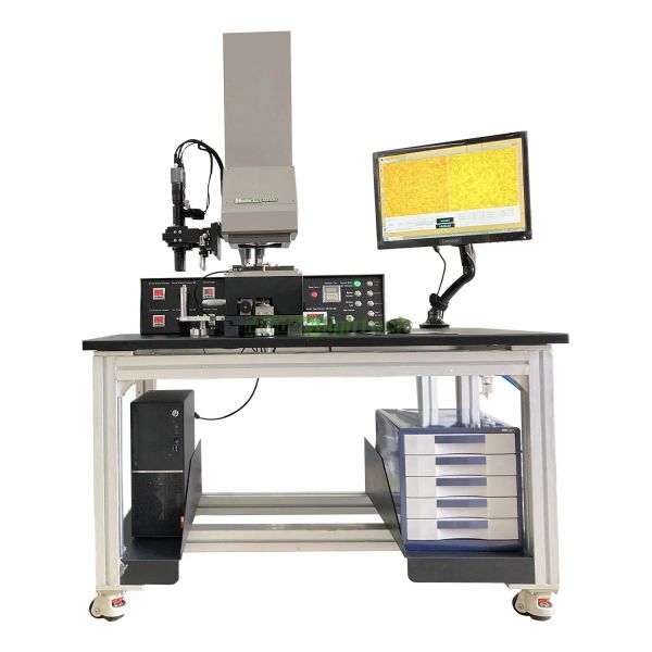
Suzhou Bozhon Semiconductor Co., Ltd
🇨🇳 China
200151-100 peopleManufacturerEstablished brand
Own brand
Product customization
Patented technology
Shipments
1
Key customer
APPLIED OPTOELECTRONICS
Key market
North America
Description
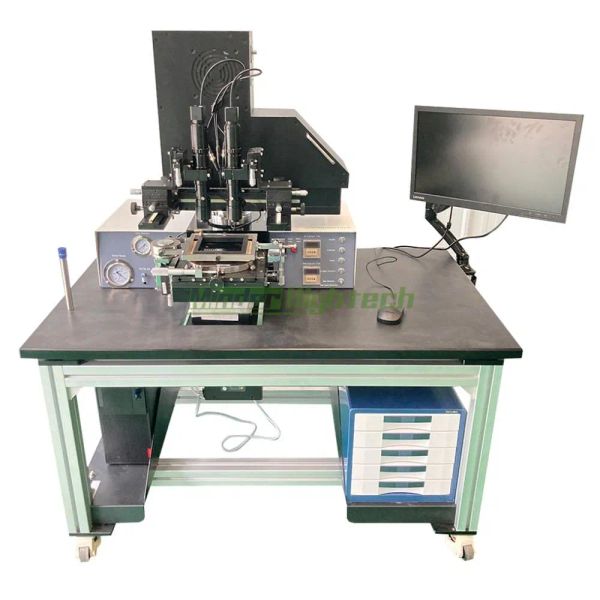
Suzhou Bozhon Semiconductor Co., Ltd. is a manufacturer and contract manufacturer based in Suzhou, China, established in 2001. As a subsidiary of Bozhon Precision Technology Co., Ltd. (stock code: 688097), the company leverages over 20 years of technological expertise in intelligent manufacturing. With 51 to 100 employees and a production base covering 400,000 m, Suzhou Bozhon Semiconductor specializes in advanced semiconductor manufacturing equipment. Their core product lines include high-speed, high-precision epoxy die bonders (FastStar Series), fully automatic high-precision eutectic die bonding machines (MicroStar Series), and AOI inspection machines (CesiStar Series). These products are critical for applications in photonics, laser, power semiconductors, microwave radio frequency, and semiconductor inspection, serving industries such as consumer electronics, new energy vehicles, and critical components. The company holds ISO 9001 certification and boasts a significant R&D presence with 1583 engineers across the parent company, holding numerous intellectual property items. They are committed to promoting advanced processes and industrial upgrades in the semiconductor industry through continuous R&D and product innovation, offering both individual machines and comprehensive turn-key solutions to domestic and international clients.
Power Semiconductor High-Precision Die Bonding Equipment$100000
High Precision Dispensing Equipment for Semiconductor Packaging Solutions$250000
Semiconductor Fully Automatic High-Precision 3D Optical Hexahedral Detection Equipment$100000
Domestic Bozhong Semiconductor Fully Automatic, High-Precision, and Multifunctional Eutectic Machine Equipment$100000
Fully Automatic Optical Detection Equipment Is Compatible with Various Chip Packaging Forms$100000
Domestic Fully Automatic Multifunctional Eutectic Machine Equipment Adopts Dynamic Tool Changing$100000
High Precision Chip Bonding Equipment Applied in The Field of Optical Communication$250000
Automatic Operation Wafer Cleaning Equipment$300000
Supply Automatic High Precision Equipment$250000
Intelligent and Rapid Defect Classification of Fully Automatic Optical Aoi Detection Equipment$100000
High Precision Die Attach Equipment$100000
Domestic Fully Automatic High-Precision Eutectic Machine Equipment for Mass Production$100000
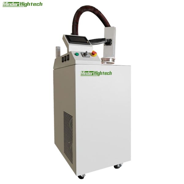
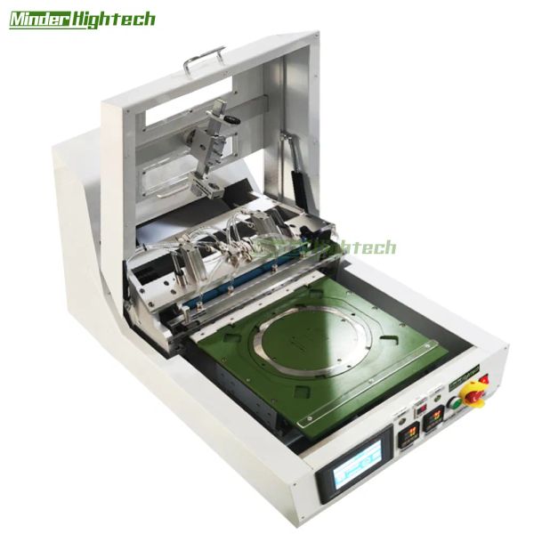
Guangzhou Minder-Hightech Co., Ltd.
🇨🇳 China
2014101-200 peopleManufacturer/Trading Company/Distributor/WholesalerProduct customization
Own brand
Low MOQ
ODM manufacturer
Shipments
561
Key customer
POLARIUM
Key market
🇻🇳 Vietnam
Description
Guangzhou Minder-Hightech Co., Ltd., also known as MinderPack, is a professional manufacturer and service representative established in 2014 and based in Guangzhou, China. The company specializes in providing one-stop machinery and engineering solutions for the semiconductor, electronic assembly, and battery production industries. Leveraging over 20 years of technical expertise in welding and connection technologies, the company serves a global clientele including major industrialized markets in North America and Europe.
Their comprehensive product portfolio covers both front-end and back-end semiconductor manufacturing, including mask aligners, wafer grinders, dicing saws, and lithography machines. They are a leading provider of IC/TO packaging equipment, such as die bonders, wire bonders, and laser solder ball placement systems. Additionally, the company offers advanced plasma surface treatment machines, vacuum reflow ovens, and helium leak detectors. For the electronics and battery sectors, they provide ultrasonic metal welders, capacitor winding machines, battery pack production lines, and automated soldering, dispensing, and screwing robots.
Operating with a team of highly educated specialists and experienced engineers, Guangzhou Minder-Hightech maintains a machining workshop for fixture design, production, and sampling. They offer both standard machinery and customized ODM solutions to help customers improve efficiency and product quality. The company holds CE certification and has established professional relationships with industry leaders such as Bosch, K&S, and TPT, as well as various scientific research institutions to stay at the forefront of technological innovation.
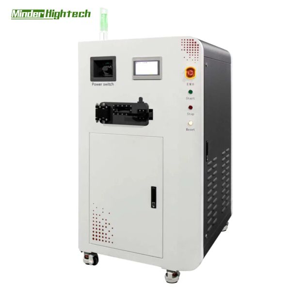
Semiconductor Chip Manufacturing Equipment Silicon Carbide Etching Rie Plasma Glue Remover$220000
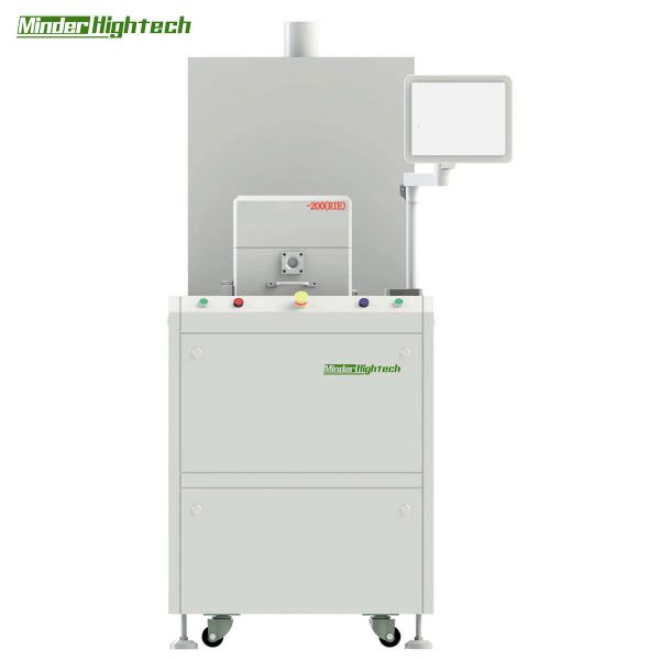
Semiconductor Research Manufacturing Equipment Material Etching Deposition Rie Reaction Ion Etching Machine$280000
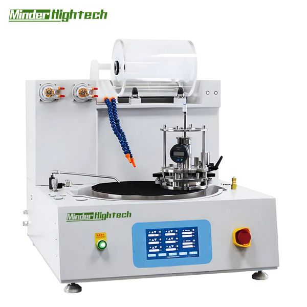
Semiconductor Wafer Manufacturer Machine Precision Flat Surface Fine Lapping Polisher$50000
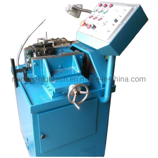
Semiconductor Device Fab Crystal Semiconductor Square Bar Rounding Forming Grinding Machine Magnetic Equipment$2300
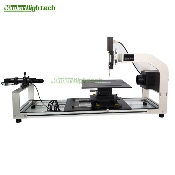
Semiconductor Manufacturing High-Precision Contact Angle Measuring Device Optical Contact Angle Tester$4000
Beol Semiconductor Device Fabrication Fab Wafer Fabrication Semiconductor Industry Equipments Mdxn-31d2 Mask Aligner$41000
Semiconductor Manufacture Welding Line Inspection Equipment Wire Bonding Wire Bonder Automatic Optical Inspect Wafer Aoi$999999
Golden Ball Semiconductor Ball Bonder Wedge Bonder Semiconductor Microelectronics Ball Bonder$43800
Semiconductor Chip Manufacture Photolithography Photomask Substrate Alignment Exposure Mask High Precision Mask Aligner$41000
Performance Testing of Semiconductor$33000
Semiconductor Equipment Automatic Wafer Mounter Dicing Saw$9999

Semiconductor Thermal Cycling Test System$33000
Shenzhen Eton Automation Equipment Co., Ltd.
🇨🇳 China
2011501-1000 peopleManufacturer/Trading CompanyHigh capacity factory
OEM manufacturer
Own brand
Product customization
Shipments
354
Key customer
GM NEXUS
Key market
🇮🇳 India
Description
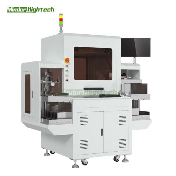
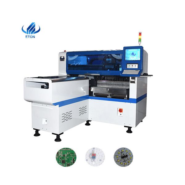
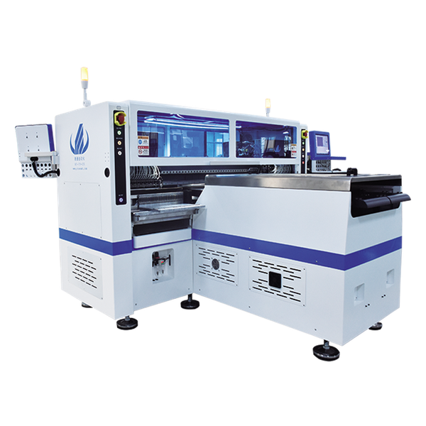
Shenzhen Eton Automation Equipment Co., Ltd. is a leading high-tech manufacturer and Industry 4.0 pioneer specializing in Surface Mount Technology (SMT) and intelligent manufacturing solutions. Established in 2011 and headquartered in Shenzhen, the company operates a massive 52,000-square-meter industrial park and employs between 500 and 1,000 professionals. Eton is recognized as a national 'Little Giant' enterprise, holding over 130 patents and numerous certifications including CE, ISO 9001, RoHS, and FCC. The company maintains a high vertical integration rate, manufacturing approximately 90% of its components in-house.
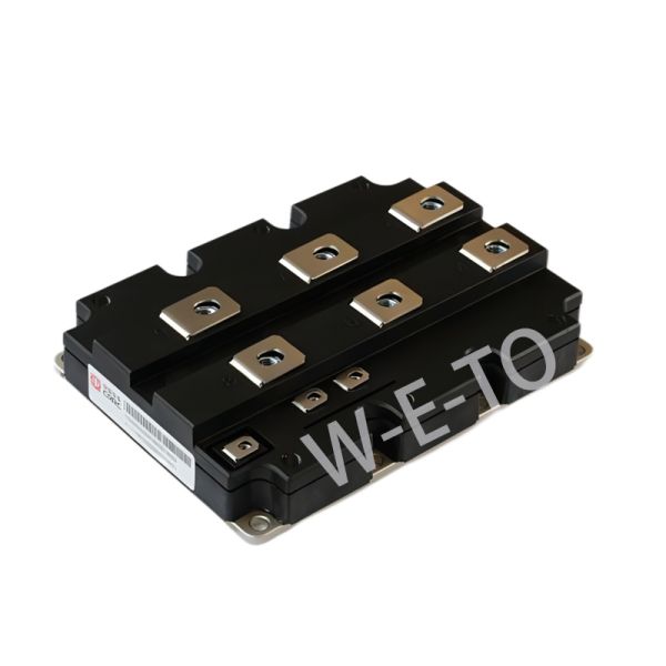
The company's core expertise lies in the R&D and production of high-speed pick and place machines, including specialized equipment for LED lighting, semiconductors, and flexible PCB assembly. Their product portfolio features the Glory series mounters, high-precision stencil printers, reflow ovens, glue dispensers, and automated optical inspection (AOI) systems. Notably, Eton has developed industry-leading technology capable of reaching speeds up to 250,000 CPH and handling components as small as 0201. They provide full turnkey SMT production line solutions for diverse sectors, including consumer electronics, automotive, aerospace, and medical devices.
With a strong international presence, Eton exports to over 30 countries and regions, including the United States, Germany, India, and Turkey. The company supports its global clientele through a network of overseas offices and local engineering teams, serving major brands such as Philips, TCL, Skyworth, and BYD. Their business model encompasses OEM and ODM services, supported by a dedicated R&D team with extensive experience in automation and precision engineering.
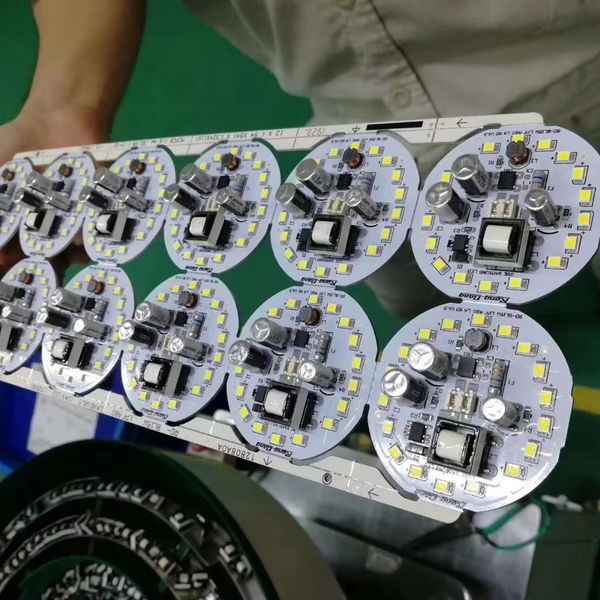
Led Light Manufacturing Machine IC Resistor Capacitors High Capacity Led Light Making Machine Automatic$78000
Magnetic Linear Motor Fully Automatic Led Light Bulb Making Machine for Ceiling Light Provided Turkey,india 0.5-5mm$43000
SMT PICK and PLACE MACHINE for RGB STRIP LIGHT MAKING$67000
How many suppliers does SourceReady track globally?
SourceReady tracks 4.0M+ suppliers globally across 200 sourcing countries and 7,000+ product categories.
Zhengzhou Shine Smart Equipment.,Ltd
🇨🇳 China
201611-50 peopleManufacturer/Service CompanyProduct customization
Low MOQ
High-tech enterprise
OEM manufacturer
Shipments
43
Key customer
AMEDA
Key market
South America
Review
5
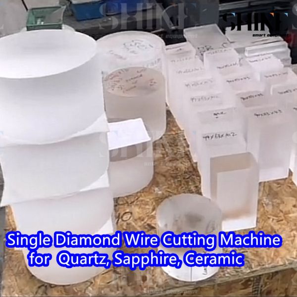
Advanced Diamond Wire Saw Blade for Multi-Purpose Cutting of Microcrystalline Glass$12000
Lianyungang Huoyun Quartz Technology Co., Ltd.
🇨🇳 China
202311-50 peopleManufacturer/Trading CompanyOEM manufacturer
Product customization
Low MOQ
High-tech enterprise
Shipments
62
Key customer
LABQUARTZ
Key market
🇮🇳 India
Review
4.2
HUOYUN Manufacture Factory Customized Heat Resistant Fused Silica Quartz Glass Plate Quartz Glass Slab$1.5
HUOYUN Manufacture Supply High Quality clear Quartz Glass Plate Heat Resistant Customized Pure Flat Glass Plate$11
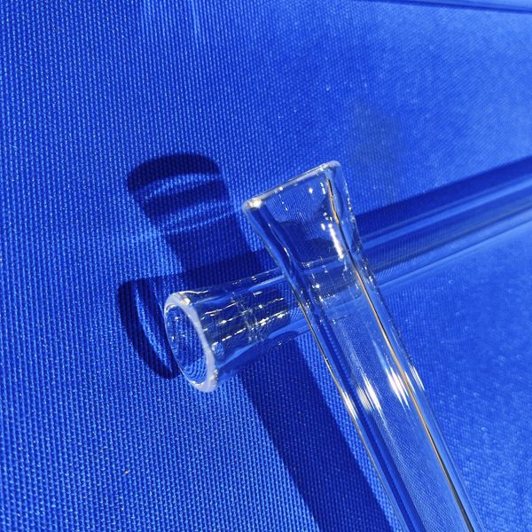
Huoyun Custom High Transparency Quartz Boat Experimental Equipment Quartz Glass Boat Quartz Ships$1
HUOYUN 150ml Laboratory Branch Pipe With Ball Experimental Equipment Professional tool$20
HY6X12 Similar to GE214 Oil burner Glass Pipe OD X THK X L 12mmx3mmx1240mm 10pc$4
Huoyun High Purify Customized Lab Bet Sample Quartz Tube Clear Hollow Quartz Ball Blowing Frosted Quartz Tubes$4
HUOYUN High Temperature and Corrosion Resistant Quartz Beaker for Chemical Experiments Quartz Glass Flask$6.5
HY Wholesaler Supply Custom Optical Quartz Rod and Refractory Quartz Rods 1 Piece High Temperature Resistant$0.42
HY Customized Heat Resistance Long and Thin Polished Crystal Clear Fused Silica Quartz Rod Clear Quartz Glass$0.38
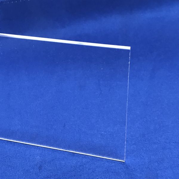
HUOYUN Factory Direct Sale clear High Temperature Resistance Glass Slabs Fused Silica Quartz Disc$1
HY Factory Customized Heat Resistant High Quality Laboratory Instrument Corrosion Resistance Quartz Instrument$0.5
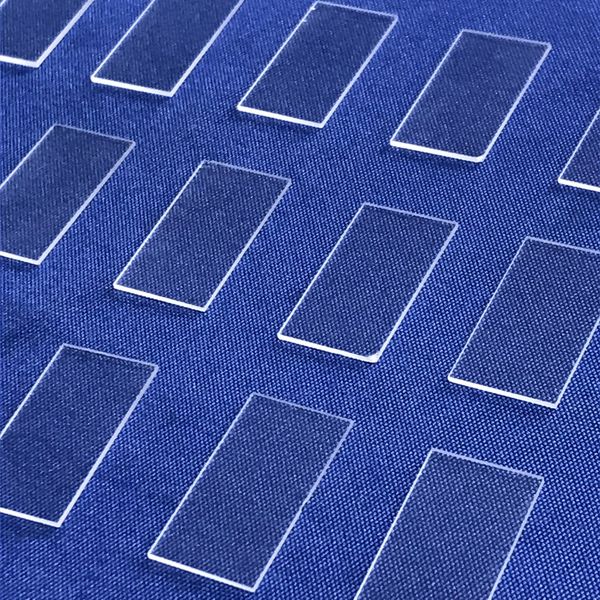
Zhejiang Advanced Quartz Technology Co., Ltd.
🇨🇳 China
199751-100 peopleManufacturer/Trading CompanyEstablished brand
OEM manufacturer
ODM manufacturer
Product customization
Shipments
47
Key customer
BOVIET SOLAR
Key market
🇸🇬 Singapore
Description
Zhejiang Advanced Quartz Technology Co., Ltd. is a manufacturer and trading company based in Huzhou, China, specializing in high-purity quartz glass products. Established in 1997, the company employs 51 to 100 people, including a technical team with over 20 years of experience in quartz deep processing. They operate a factory spanning approximately 7,500 square meters, utilizing advanced processing equipment such as glass forming lathes, CNC machines, water jet cutters, and laser machines. Zhejiang Advanced Quartz Technology offers OEM and ODM services and is certified with ISO 9001 and ISO 14001. Their comprehensive product portfolio includes quartz boats, tubes, instruments, plates, wafers, tanks, crucibles, furnace doors, rings, injectors, bell jars, capillary tubes, beakers, heaters, and sheaths. These products are primarily designed for the 4-12 inch Integrated Circuit Industry, solar cell manufacturing, scientific experiments, medical, and laboratory analysis sectors. The company sources high-quality materials from Momentive, Heraeus, and China Pacific. With a strong international presence, 60% of their products are exported to over 12 countries, including the United States, Germany, UK, France, Singapore, Malaysia, Vietnam, Cambodia, India, and Taiwan, China.
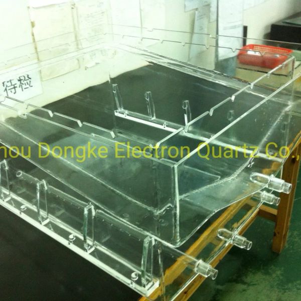
Cleaning Tank, Quartz Bath$500
Beijing World E To Technology Co., Ltd.
🇨🇳 China
201511-50 peopleManufacturer/Trading Company/DistributorOEM manufacturer
ODM manufacturer
Product customization
Low MOQ
Shipments
930
Key customer
KYOKUTO BOEKI KAISHA MEXICO
Key market
🇲🇽 Mexico
Description
Beijing World E To Technology Co., Ltd. is a Beijing-based technology company specializing in semiconductor solutions, power electronics, and industrial components. Operating as a manufacturer, distributor, and contract manufacturer with ISO 9001 certification, the company serves as an official agent for major industry leaders including CRRC, STARPOWER, PERI, and HUAWEI. The firm is a specialist in semiconductor alternative solutions, focusing on improving supply chain security and cost-performance through high-quality Chinese-made components.
MK300 300A 600V 1800V Fast Turn-Off Thyristor Modules for Inverter Inductive Heating Chopper$29
Y89KFG Fast Turn-Off Non-Symmetric Thyristor 3800A 2000~3000V VRRM 1000~2500V for Inductive Heating Self-Commutated Inverter$31
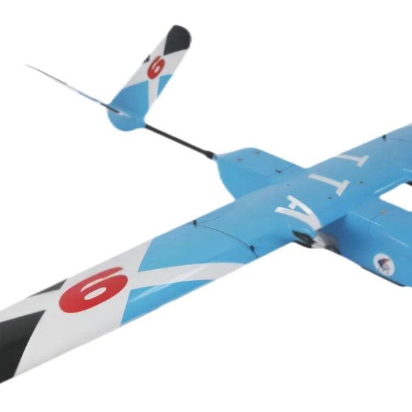
Fixed Wing Uav$500
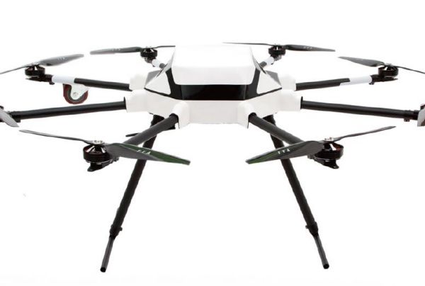
Security Uac$500
MTC200 200A 800V-1800V AC/DC Welding Thyristor Various Rectifiers DC Supply for PWM Inverter Motor Drives Various Applications$20
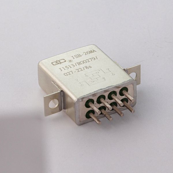
JSB-26M 1A 28Vdc Electromagnetic Relay for Timed Switching Used Aerospace National Defense Industrial Control Research Aviation$2.26
Fast Recovery Diode$1
IGBT$58
MTC160 160A 600V-1800V AC/DC Thyristor for Welding Various Rectifiers & PWM Inverter with DC Supply Motor Drives$20
IGBT$680
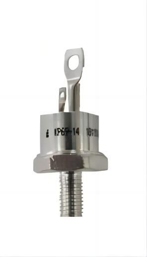
Rotating Excitation Thyristor$1
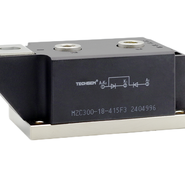
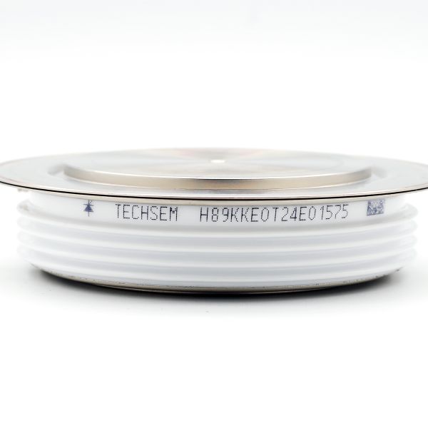
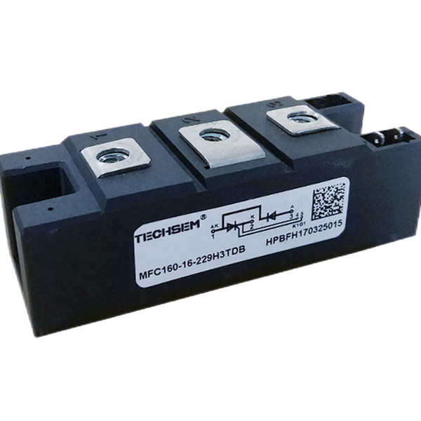
Fast Recovery Diode Modules MZx300 MZ300 300A 600V-1800V for Inverter Inductive Heating Chopper Water Cooling TECHSEM Thyristors$20
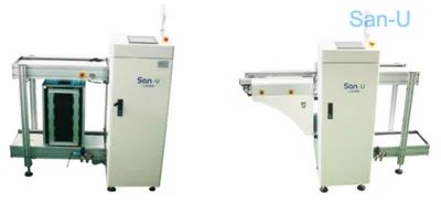
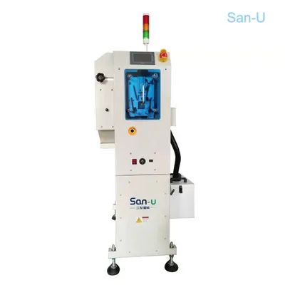
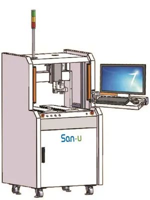
Shenzhen Sanyou Intelligent Automation Equipment Co. Ltd
🇨🇳 China
2001Fewer than 5 peopleManufacturer/Service Company/Trading CompanyEstablished brand
High-tech enterprise
Product customization
Low MOQ
Shipments
3
Key customer
SKYQUAD
Key market
🇮🇳 India
Description
Shenzhen Sanyou Intelligent Automation Equipment Co. Ltd is a national high-tech enterprise and a manufacturer of SMT supporting and related automation equipment, established in 2001. The company specializes in the research, development, manufacturing, sales, and service of a wide range of automation equipment, including SMT equipment, PCB cleaning machines, board feeders, automated optical inspection equipment, laser marking machines, semiconductor vacuum reflow welding, loaders and unloaders, aging lines, assembly lines, aging racks, and various conveyor belt systems. They offer both standard and non-standard automation solutions, with a focus on providing complete automation technology solutions and custom-made products to meet specific client requirements. With a production plant of nearly 2000 square meters and a team of skilled personnel, Shenzhen Sanyou Intelligent Automation Equipment Co. Ltd emphasizes independent innovation, quality excellence, and 24-hour technical support. The company holds certifications such as Safety Production License, 3A Integrity Enterprise, and High and New Technology Enterprise Certificate, and has completed international trades, exporting machinery for PCB assembly.
Solder Paste Inspection Equipment
SMT Automatic PCB Loader and Unloader for SMT
SMT Automatic PCB Cleaning Machine
Dispenser Machine
Edwards Vacuum
🇬🇧 United Kingdom
20075001-10000 peopleManufacturer/Service CompanyHigh capacity factory
Large enterprise group
Multinational enterprise
Eco-friendly supplier
Shipments
3341
Key customer
EDINTEL
Key market
🇨🇷 Costa Rica
Description
Edwards Vacuum, a global leader in vacuum and abatement solutions, is a manufacturer and service company based in Burgess Hill, UK, with a significant global presence and operations as part of the Atlas Copco Group. Established with between 5,001 and 10,000 employees, the company specializes in providing comprehensive vacuum, abatement, and service solutions for a broad range of industries, including semiconductor manufacturing, general industries, and research & development. Their extensive product portfolio includes dry pumps, turbomolecular pumps, oil-sealed pumps, diffusion pumps, liquid ring pumps, chemical dry pumps, mechanical boosters, vacuum valves, fittings, exhaust management systems, vacuum gauges, and residual gas analyzers. Edwards Vacuum offers OEM and ODM services and is expanding its manufacturing capabilities, including a new $319 million facility in Genesee County, New York, to produce dry pumps for the semiconductor industry, aiming for LEED certification. The company emphasizes innovation, sustainability, and customer partnership, providing services such as accredited calibration, exchange pump replacement, certified used pumps, service plans, and remote monitoring through GENIUS Instant Insights. They serve diverse sectors including Analytical Instruments, Carbon Capture, Chemical Processing, Display, Energy Solutions, Food Processing, Metallurgy, Plastics & Composites, Thin Film Coating, and TVAC Testing in Space Qualification, with a strong commitment to reducing environmental impact.
FAQ
Can enterprise teams use SourceReady for supplier research?
What information should I check before contacting a supplier?
Can I import my own suppliers into SourceReady?