Advanced Compound Semiconductors (Beijing) Co., Ltd.
Similar suppliers you may like

Advanced Semiconductor Materials Co., Ltd.
🇨🇳 China
201911-50 peopleManufacturerOwn brand
Product customization
Low MOQ
ODM manufacturer
Shipments
3
Key customer
ASCENX
Key market
North America
Description
Advanced Semiconductor Materials Co., Ltd. (ASMC) is a manufacturer and ODM provider based in Jinan, China, specializing in advanced wide band gap semiconductor materials. Established in 2012, ASMC is a branch of Suzhou Nanowin Science and Technology Co., Ltd. The company employs 11-50 people and focuses on developing and manufacturing high-quality, cost-effective materials such as Gallium Nitride (GaN), Silicon Carbide (SiC), Aluminium Nitride (AlN), and Diamond single crystal substrates and epi wafers. Their product portfolio includes 2-6 inch free-standing GaN substrates, 2-8 inch standard GaN epitaxial wafers, customized epitaxial wafers for PIN/SBD/HEMT/MOS/LED, 2-inch free-standing AlN substrates, 2-4 inch AlN epitaxial wafers, 4-6 inch high-quality semi-insulating SiC substrates, 4-6 inch SiC epi substrates, and 10x10mm single crystal or polycrystalline diamond (optical/electronic grade). ASMC also offers customized MicroLED chips, screens, and panels, along with semiconductor equipment and consumables like quartz, fused silica, sapphire, PECVD SiC, and PECVD GaN. The company holds certifications including IATF 16949, ISO 9001, ISO 14001, ISO 14000, OHSAS/OHSMS 18001, and QC 080000, demonstrating a commitment to quality and environmental management. With over 10 production lines and an annual output value exceeding US$100 Million, ASMC is dedicated to providing competitive "created in China" third-generation semiconductor sources.
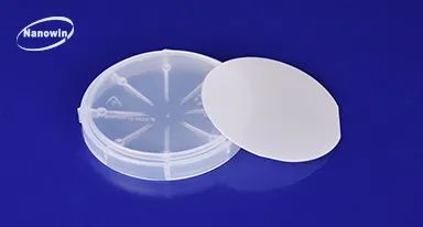
Nanowin GaN Epitaxial Wafers / GaN on Sic (GaN/SiC)
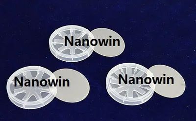
Nanowin 2~4 Inch Free-Standing GaN Substrates (Gallium Nitride) /U-GaN, N-GaN, Si-GaN
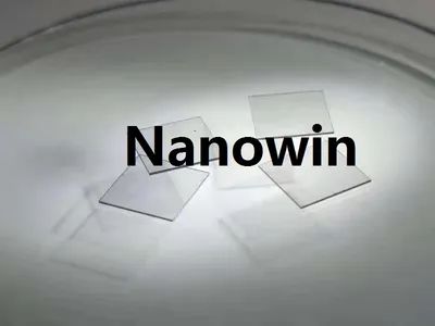
Nanowin 10mm*10mm Small Pieces Diamond Single Crystal Substrate
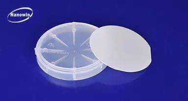
Nanowin GaN Epitaxial Wafers / GaN on Customized Substrate (customized structure)
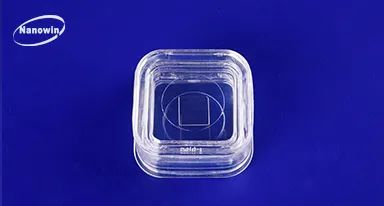
Nanowin 10mm*10.5mm Small Pieces of Free-Standing GaN Substrates (Customized size, Un-doped, Si-doped, Fe-doped)
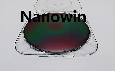
Nanowin 4~8 Inch GaN Epitaxial Wafers/GaN Epi Wafers/ GaN on Si/ GaN on Sic/ GaN on GaN/ GaN on Sapphire
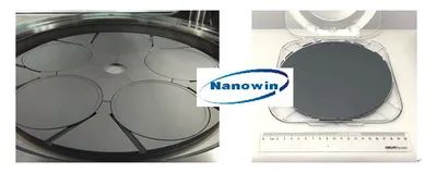
Nanowin 4~6 Inch GaN Epitaxial Wafers/GaN Epi Wafers/GaN Templates (GaN on Si/ GaN on SiC/ GaN on GaN/ GaN on Sapphire)
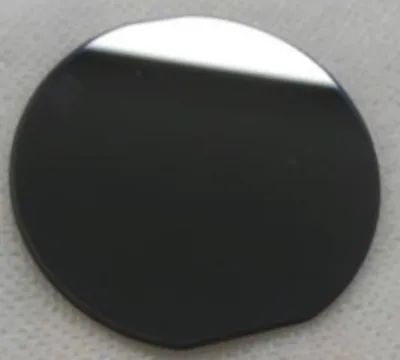
2 Inch CVD Wafer Level Diamond Wafers / Diamond Heat Sink

Beijing Boyu Semiconductor Vessel Craftwork Technology Co., Ltd.
🇨🇳 China
2002301-500 peopleManufacturerEstablished brand
OEM manufacturer
Product customization
Patented technology
Shipments
3
Key customer
DELOITTE
Key market
South America
Description
Beijing Boyu Semiconductor Vessel Craftwork Technology Co., Ltd., established in 2002, is a leading manufacturer of ultra-high purity pyrolytic boron nitride (PBN) and pyrolytic graphite (PG) products based in Beijing, China. As the first large-scale PBN manufacturing enterprise in China, the company specializes in the design, development, production, and sales of CVD products. With over 310 employees and a new production base capable of 100,000 units per year, Boyu Semiconductor holds a dominant position in the domestic market and is globally leading in PBN production capacity and market share. The company is an ISO 9001 certified high-tech enterprise, authorized by the Beijing government, with a core team of material scientists from the Chinese Academy of Sciences, holding over 20 patents. They offer a comprehensive range of products including PBN crucibles (OLED, MBE, VGF, LEC), PBN boats, rods, rings, machined parts, and coatings, as well as PG crucibles, plates, and PBN-PG-PBN composite heaters. Additionally, they provide refractory metal products like tantalum, tungsten molybdenum, and titanium crucibles, and other ceramics such as aluminum nitride, aluminum oxide, and boron nitride crucibles. These products are critical for advanced technology fields including OLED production, molecular beam epitaxy (MBE), semiconductor crystal growth, polycrystal synthesis, MOCVD heaters, 5G communication, AR/VR, and aerospace. Boyu Semiconductor also offers OEM services and exports to international markets including Europe, America, Japan, Korea, Singapore, and Taiwan.
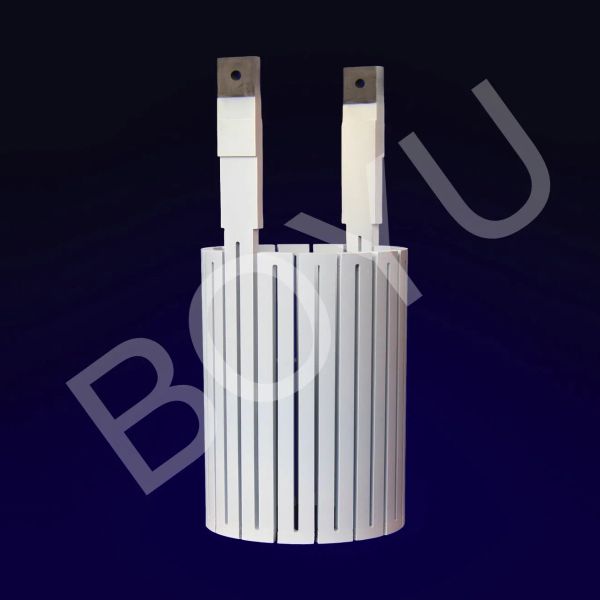
Boyu High Purity 99.999% Pbn Coating$400
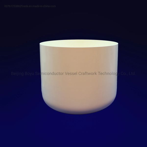
Boyu Competitive Price Liquid Encapsulation Czochralsk Crucible$400
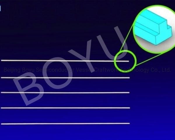
Boyu High Purity 99.999% Pbn Rod$400
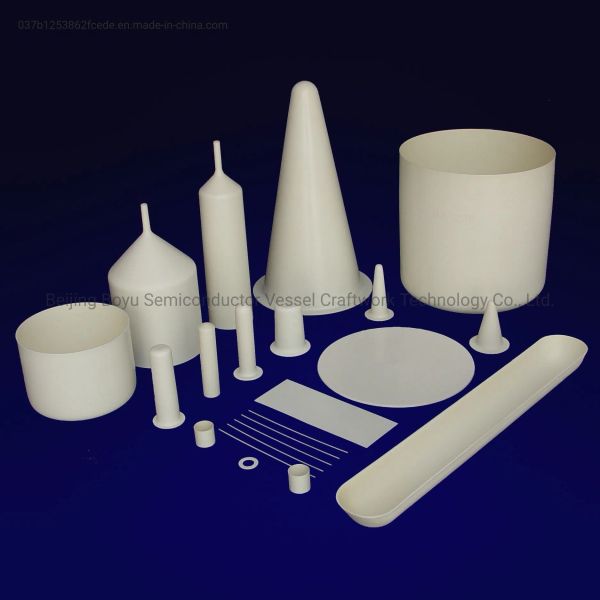
Boyu Lec Crucible Is Applied as Vessel of Crystal Growth in Lec$400
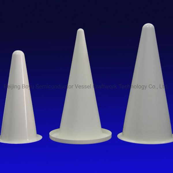
Pbn Crucible That Customizable for Mbe$400
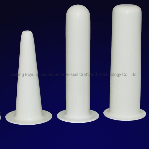
High Purity (5N) Molecular Beam Epitaxy Crucible for Crystal Epitaxial Growth$400
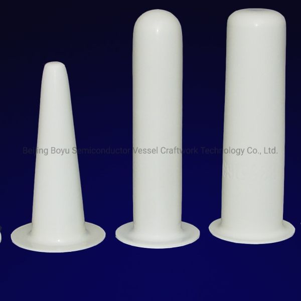
High Purity (5N) Mbe Crucible for Crystal Epitaxial Growth$400
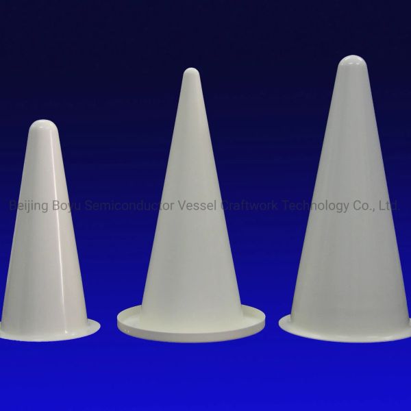
Mbe Crucible for Crystal Epitaxial Growth$400
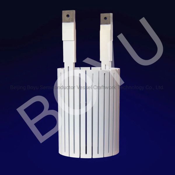
High Purity 99.999% Pbn Coating$400
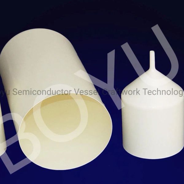
The Leader of Vgf Pbn Crucible$400
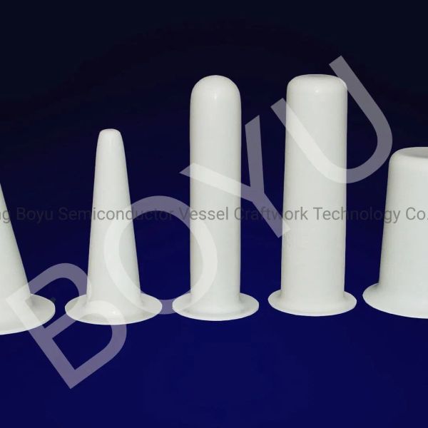
High Purity (99.999%) / Low Outgassing in High Temperature/ Excellent Thermal Conductivity and Shock Resistance Mbe Pbn Crucible$400
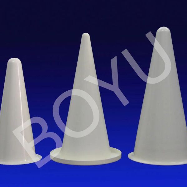
High Purity (99.999%) Mbe Crucible for Crystal Epitaxial Growth$400


