Advanced Semiconductor Materials Co., Ltd.

Advanced Semiconductor Materials Co., Ltd.
🇨🇳 China, Shandong
201911-50 peopleManufacturerAdvanced Semiconductor Materials Co., Ltd. (ASMC) is a manufacturer and ODM provider based in Jinan, China, specializing in advanced wide band gap semiconductor materials. Established in 2012, ASMC is a branch of Suzhou Nanowin Science and Technology Co., Ltd. The company employs 11-50 people and focuses on developing and manufacturing high-quality, cost-effective materials such as Gallium Nitride (GaN), Silicon Carbide (SiC), Aluminium Nitride (AlN), and Diamond single crystal substrates and epi wafers. Their product portfolio includes 2-6 inch free-standing GaN substrates, 2-8 inch standard GaN epitaxial wafers, customized epitaxial wafers for PIN/SBD/HEMT/MOS/LED, 2-inch free-standing AlN substrates, 2-4 inch AlN epitaxial wafers, 4-6 inch high-quality semi-insulating SiC substrates, 4-6 inch SiC epi substrates, and 10x10mm single crystal or polycrystalline diamond (optical/electronic grade). ASMC also offers customized MicroLED chips, screens, and panels, along with semiconductor equipment and consumables like quartz, fused silica, sapphire, PECVD SiC, and PECVD GaN. The company holds certifications including IATF 16949, ISO 9001, ISO 14001, ISO 14000, OHSAS/OHSMS 18001, and QC 080000, demonstrating a commitment to quality and environmental management. With over 10 production lines and an annual output value exceeding US$100 Million, ASMC is dedicated to providing competitive "created in China" third-generation semiconductor sources.
ODM manufacturerProvides ODM design and manufacturing solutions.
Own brandOwns and operates its own brands and manufacturing facilities.
Product customizationOffers full customization for design and features.
Low MOQOffers low minimum order quantity options.
Contact
No contact yet
Products
Products
0
Categories
0
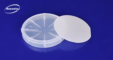
Nanowin GaN Epitaxial Wafers / GaN on Sic (GaN/SiC)
0·0 reviews
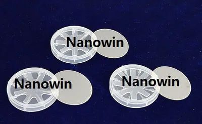
Nanowin 2~4 Inch Free-Standing GaN Substrates (Gallium Nitride) /U-GaN, N-GaN, Si-GaN
0·0 reviews

Nanowin 10mm*10mm Small Pieces Diamond Single Crystal Substrate
0·0 reviews
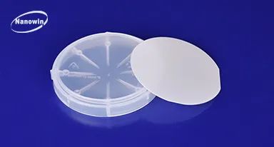
Nanowin GaN Epitaxial Wafers / GaN on Customized Substrate (customized structure)
0·0 reviews
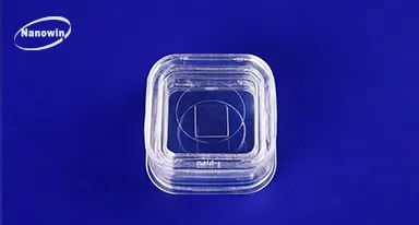
Nanowin 10mm*10.5mm Small Pieces of Free-Standing GaN Substrates (Customized size, Un-doped, Si-doped, Fe-doped)
0·0 reviews
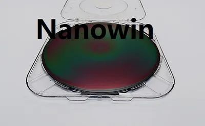
Nanowin 4~8 Inch GaN Epitaxial Wafers/GaN Epi Wafers/ GaN on Si/ GaN on Sic/ GaN on GaN/ GaN on Sapphire
0·0 reviews
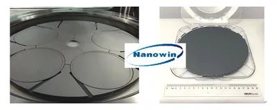
Nanowin 4~6 Inch GaN Epitaxial Wafers/GaN Epi Wafers/GaN Templates (GaN on Si/ GaN on SiC/ GaN on GaN/ GaN on Sapphire)
0·0 reviews
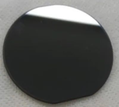
2 Inch CVD Wafer Level Diamond Wafers / Diamond Heat Sink
0·0 reviews
Customers
ASCENX
Certifications
 IATF 16949
1
 ISO 9001
1
 ISO 14001
1
Ask AI about this supplier
Key export market
Shipments
Shipments count
0
Export volume
0 kg
Export countries
0
Customers
0
Insights
Top 5 customers
Reflecting the depth of cooperation between supplier and customersTop 5 customers
This insight is only available in the Pro planTop 5 export countries
Reflecting the supplier's export experience in target countriesTop 5 export countries
This insight is only available in the Pro planShipment count distribution
Reflecting the supplier's market business activityAll categories
Shipment count distribution
This insight is only available in the Pro planExport weight distribution (kg)
Reflecting the supplier's export scaleAll categories
Export weight distribution (kg)
This insight is only available in the Pro planExport weight trend (kg)
Reflecting the growth rate of the supplier's phased total supply volume and the fluctuation of supply volume, identifying supply peaks and troughsAll categories
Export weight trend (kg)
This insight is only available in the Pro planCIF trend (USD)
For identifying high-value cooperation periods and single order value changesAll categories
CIF trend (USD)
This insight is only available in the Pro planSimilar suppliers you may like
Advanced Compound Semiconductors (Beijing) Co., Ltd.
🇨🇳 China
201411-50 peopleManufacturerHigh-tech enterprise
Patented technology
Low MOQ
Product customization
Description
Advanced Compound Semiconductors (Beijing) Co., Ltd., founded in October 2014, is a specialized manufacturer of III-V compound semiconductor materials for microelectronics and optoelectronics. Based in Beijing, China, the company operates the nation's first large-scale production base for gallium arsenide (GaAs) molecular beam epitaxy (MBE) with independent intellectual property rights. The facility features advanced Veeco Gen2000 and Gen200 MBE systems, world-class analysis and testing equipment, and ultra-clean dust-free workshops ranging from class 10 to 1000.
The company specializes in the research, development, and production of high-performance epitaxial wafers, including GaAs and Indium Phosphide (InP) substrates. Its extensive product portfolio features PHEMT and HEMT epiwafers for radio frequency applications, VCSEL epiwafers for optoelectronics, and various other specialized materials such as HBT, BiHEMT, laser, photodetector, and LED epiwafers. These products are critical components for RF chips, face ID technology, mobile communications (4G/5G), base stations, optical fiber communications, and aerospace applications.
With a current production capacity of 60,000 to 80,000 6-inch GaAs epitaxial chips annually and a future target exceeding 500,000 pieces, the company serves international markets in semiconductor processing, defense, and advanced manufacturing. Advanced Compound Semiconductors (Beijing) Co., Ltd. is a certified National High-tech Enterprise and holds ISO 9001:2015 and ISO 14001 certifications, ensuring its products meet international standards for electron mobility, surface defect density, and material homogeneity.
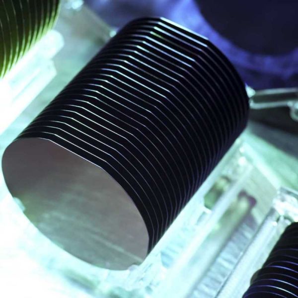
Custom 2-6 Inch GaAs/Inp Epi Wafers$150
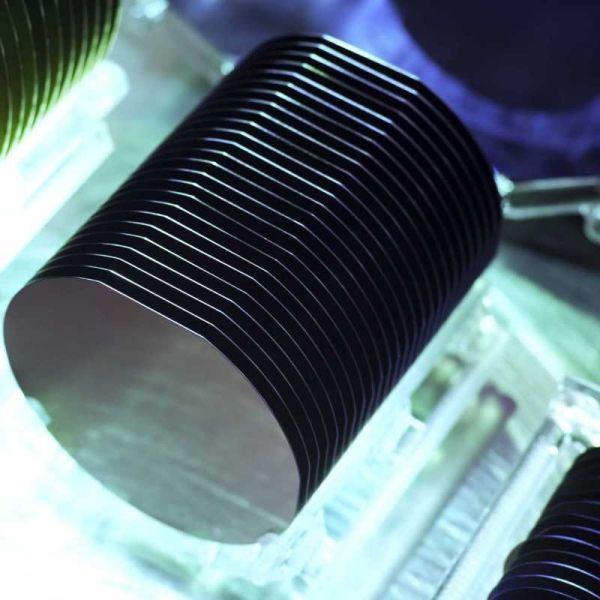
Custom GaAs Photocathode Epi Wafers$100
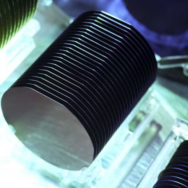
Custom 2-4 Inch Inp Epi Wafers$300

Shandong Tian Yue Advanced Material Technology Co., Ltd.
🇨🇳 China
201111-50 peopleManufacturer/Trading CompanyHigh-tech enterprise
Low MOQ
Own brand
Key customer
BOSCH
Key market
Asia
Description
Shandong Tian Yue Advanced Material Technology Co., Ltd. is a high-tech manufacturer and trading company based in Jinan, China, specializing in advanced semiconductor materials. Established in 2011, the company employs 11 to 50 people and operates a factory focused on the growth and mechanical treatment of sapphire and SiC crystals. They are a leading provider of single crystal silicon carbide substrates, offering conductive and semi-insulating SiC substrates, as well as 2"-6" sapphire wafers and 2"-4" SiC wafers. Their products, including Epi-ready Sapphire and SiC wafers, are widely utilized in semiconductor light-emitting diodes (LEDs), high-power, and high-frequency electronic devices. Shandong Tian Yue Advanced Material Technology Co., Ltd. is recognized for its advanced technology and management, serving customers like Bosch, and is one of the few manufacturers capable of supplying high-quality epitaxial substrates. The company has also pursued an international development strategy, including an 'A+H' listing on the Hong Kong Stock Exchange.
Alumina Feedstock$3400
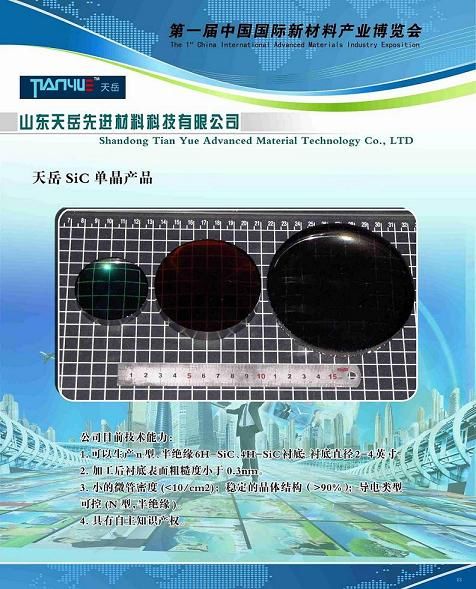
Sic Wafers$11


