Best Semiconductor Wafer Production Suppliers
Discover trusted sources for high-quality semiconductor wafers, featuring advanced materials, fabrication methods, and custom solutions to meet your specific production needs.
SemiconductorsWafersFabricationMaterials

Wuhan Xinrong New Materials Co., Ltd.
🇨🇳 China
201451-100 peopleManufacturer/Trading Company/Service CompanyProduct customization
Low MOQ
High-tech enterprise
ODM manufacturer
Key customer
ABHIMANYU METALLIC
Key market
North America
Description
Wuhan Xinrong New Materials Co., Ltd. is a specialized technology company and manufacturer established in 2014, headquartered in Wuhan, China. The company focuses on the research, development, and production of high-end high-purity metal materials, rare earth metals, and nano-materials. Operating a 3,000 to 5,000 square meter factory with ten production lines, the firm has established itself as a significant international supplier of semiconductor and thermoelectric materials. Their extensive product portfolio includes high-purity Tellurium, Germanium, Indium, Gallium, Antimony, Bismuth, Cadmium, Selenium, and Tin, with purity levels ranging from 99% to 99.999999%. They also specialize in compound materials such as Bismuth Telluride and Cadmium Telluride, as well as sputtering targets and metal powders. Wuhan Xinrong New Materials Co., Ltd. serves a global clientele across 26 countries, including the United States, United Kingdom, and Japan, and maintains partnerships with industry leaders like Heraeus and Umicore. The company is ISO 9001 and GMP certified, reflecting its commitment to quality standards. With a workforce of approximately 50 to 200 employees, including a dedicated R&D team of doctoral engineers, they offer comprehensive OEM, ODM, and customized synthesis services to high-tech enterprises and research institutes worldwide.
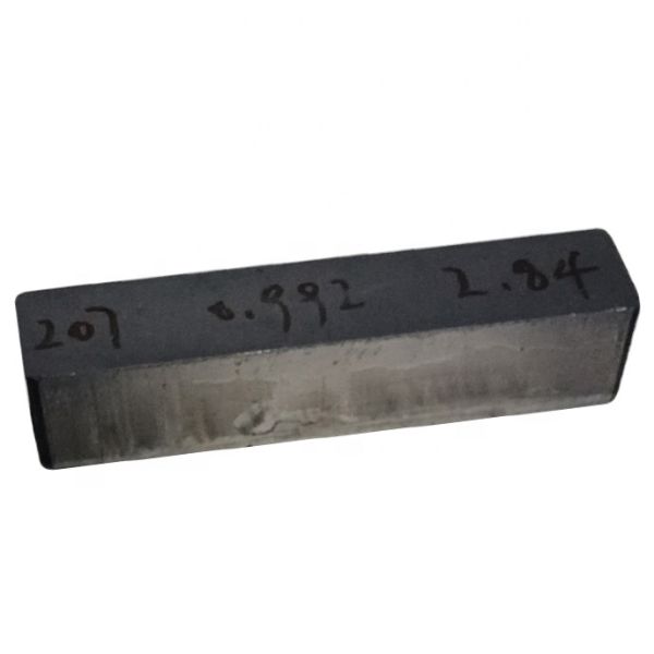
Sps P Type Thermoelectric Bismuth Telluride Semiconductor Bi2te3 Ingot$212.8
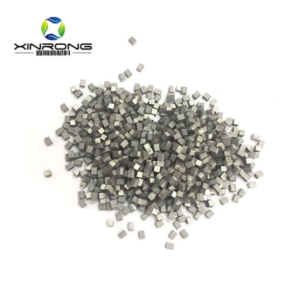
Thermoelectric Bi2te3 1.4X1.4X1.6mm N-Type P-Type Bismuth Telluride Semiconductor Pellets$357
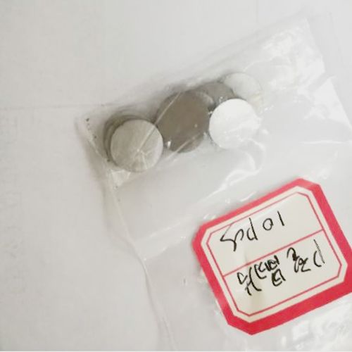
30mm P/N Type Bi2te3 Plate Bismuth Telluride Discs 99.99% Pure Bismuth Telluride Wafer$10
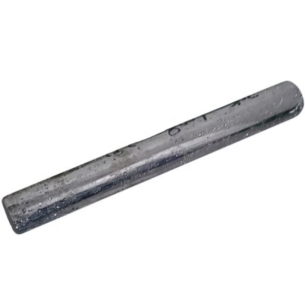
Thermoelectric Materials Bi2te3 Bismuth Telluride Rod N Type Bismuth Telluride Bar$212.8
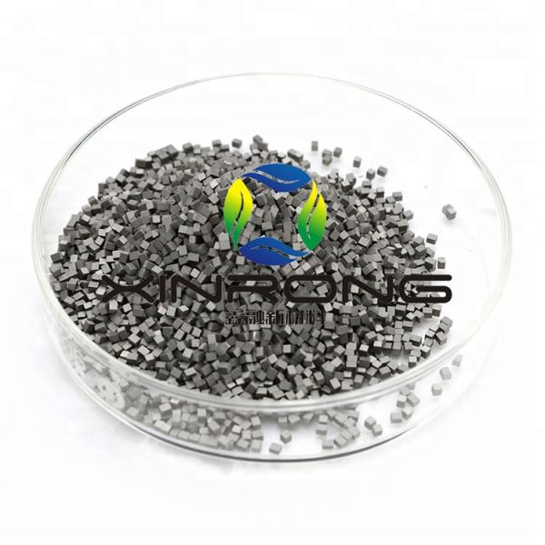
Bismuth Telluride Thermoelectric Element 1.4X1.4X1.6mm N P Type Bismuth Telluride Pellet$357
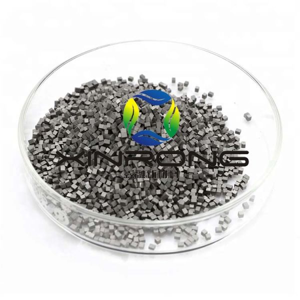
Thermoelectric Tec Teg P/N Bi2te3 N-Type P-Type Bismuth Telluride Pellet$254
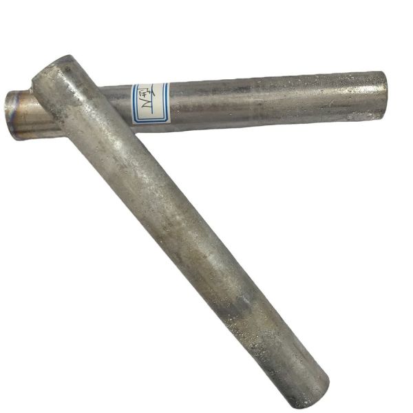
Hot Extrusion Bismuth Telluride Bars 30mm N Type Bismuth Telluride Rod$212.8
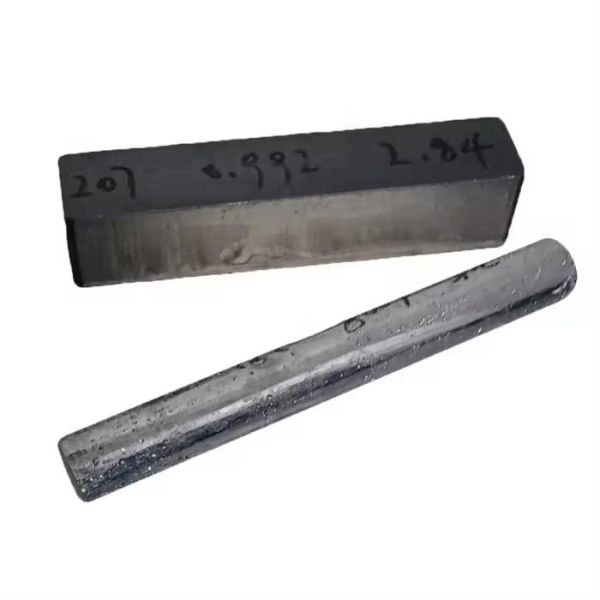
P/N Type Bi2te3 N-Type Bismuth Telluride Rod P-Type Bismuth Telluride Ingot$212.8
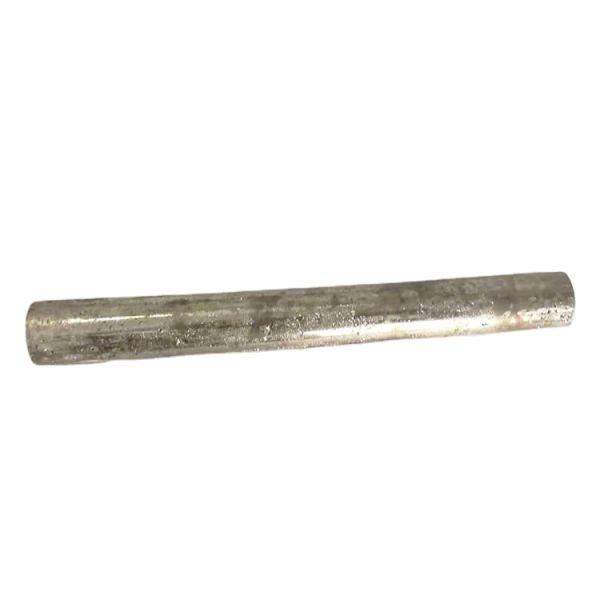
Bi2te3 P Type 30mm Bismuth Telluride Monocrystalline Rod P-Type Bismuth Telluride Rod$212.8

Guangzhou Minder-Hightech Co., Ltd.
🇨🇳 China
2014101-200 peopleManufacturer/Trading Company/Distributor/WholesalerProduct customization
Own brand
Low MOQ
ODM manufacturer
Key customer
POLARIUM
Key market
🇲🇽 Mexico
Description
Guangzhou Minder-Hightech Co., Ltd., also known as MinderPack, is a professional manufacturer and service representative established in 2014 and based in Guangzhou, China. The company specializes in providing one-stop machinery and engineering solutions for the semiconductor, electronic assembly, and battery production industries. Leveraging over 20 years of technical expertise in welding and connection technologies, the company serves a global clientele including major industrialized markets in North America and Europe.
Their comprehensive product portfolio covers both front-end and back-end semiconductor manufacturing, including mask aligners, wafer grinders, dicing saws, and lithography machines. They are a leading provider of IC/TO packaging equipment, such as die bonders, wire bonders, and laser solder ball placement systems. Additionally, the company offers advanced plasma surface treatment machines, vacuum reflow ovens, and helium leak detectors. For the electronics and battery sectors, they provide ultrasonic metal welders, capacitor winding machines, battery pack production lines, and automated soldering, dispensing, and screwing robots.
Operating with a team of highly educated specialists and experienced engineers, Guangzhou Minder-Hightech maintains a machining workshop for fixture design, production, and sampling. They offer both standard machinery and customized ODM solutions to help customers improve efficiency and product quality. The company holds CE certification and has established professional relationships with industry leaders such as Bosch, K&S, and TPT, as well as various scientific research institutions to stay at the forefront of technological innovation.

Semiconductor Wafer Cleaving Machine$99999
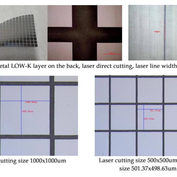
Semiconductor Wafer Stealth Laser Dicing Saw$415000
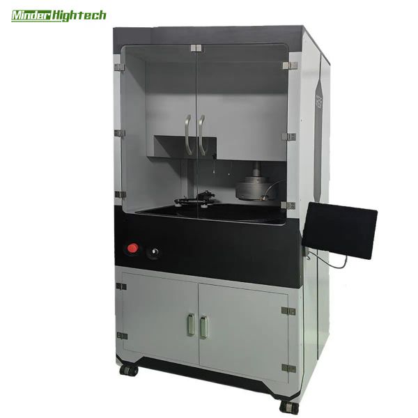
Semiconductor Wafer Surface Precision Chemical Mechanical Planarization CMP$170000
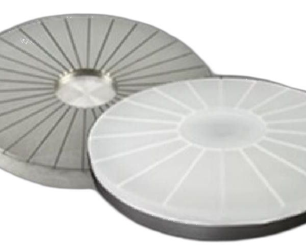
Semicon China CMP device Grinding Thinning Polishing Equipment of Semiconductor Wafer Semiconductor Material$112000
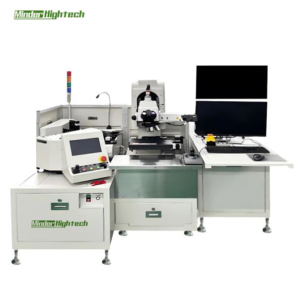
Microscopic Inspection Semiconductor Wafer Defect Detection Mdwx-Wi8100 Automatic Wafer Inspection System$240000
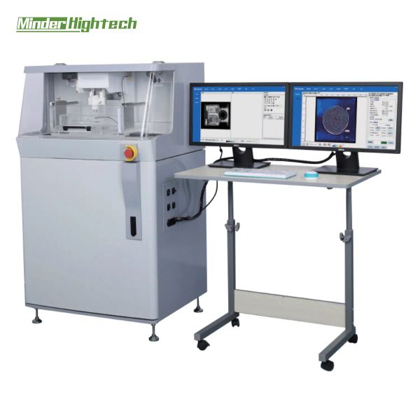
Semiconductor Wafer Chil Testing Inspecting Equipment Ultrasonic Scanning Microscope$9999
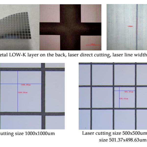
Semiconductor Wafer Stealth Laser Dicing Saw / Wafer Laser Scribing Dicing Die modification Separator$415000
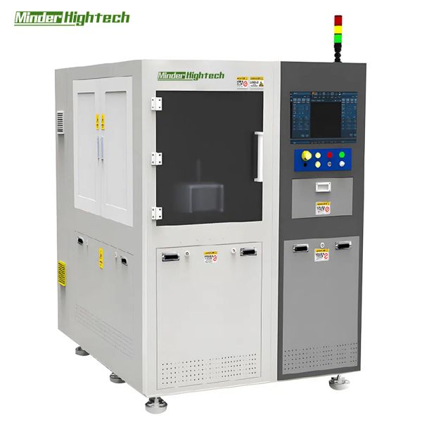
Semiconductor Wafer Laser Scribing Dicing Die Modification Separator / Wafer Stealth Laser Dicing Saw$350000
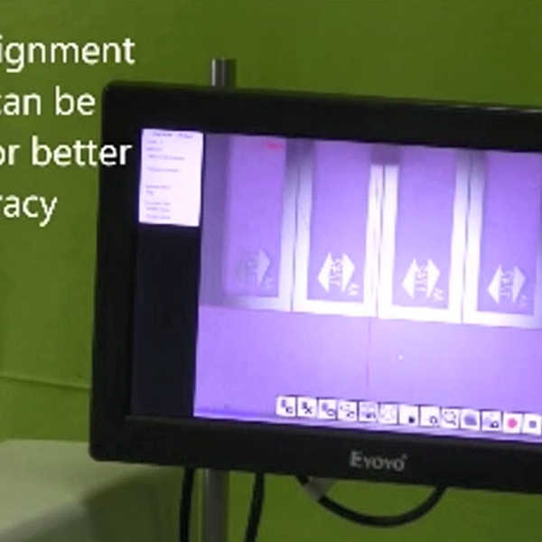
Semiconductor Wafer Substrates GaAs and Inp Scribing and Splitting Machine Manual Wafer Scriber$49000
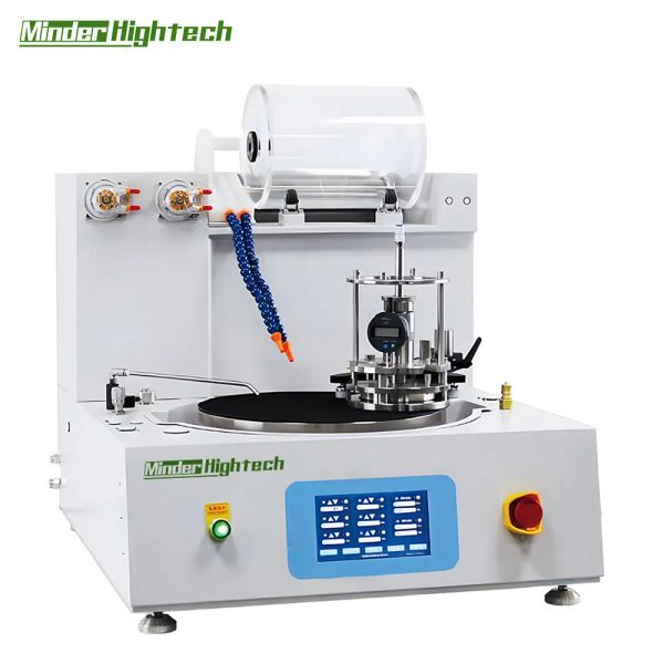
Semiconductor Wafer Manufacturer Machine Precision Flat Surface Fine Lapping Polisher$50000
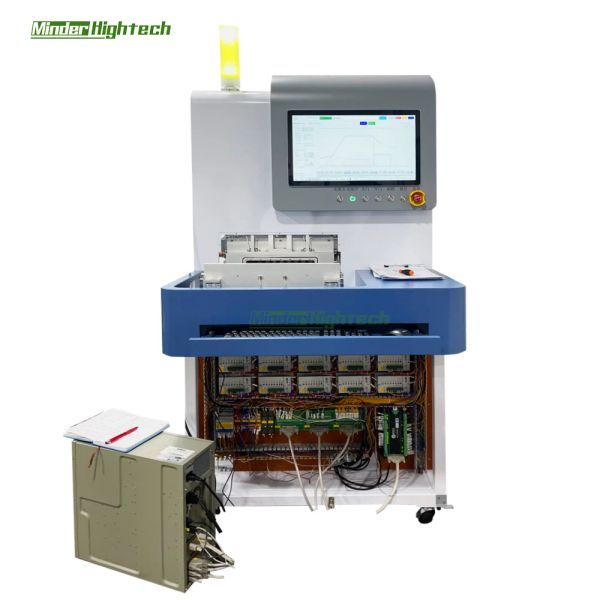
Semiconductor Wafer Fab Fabrication Desktop Rapid Thermal Processing RTP equipment for compound semiconductors SlC LED and MEMS$999999
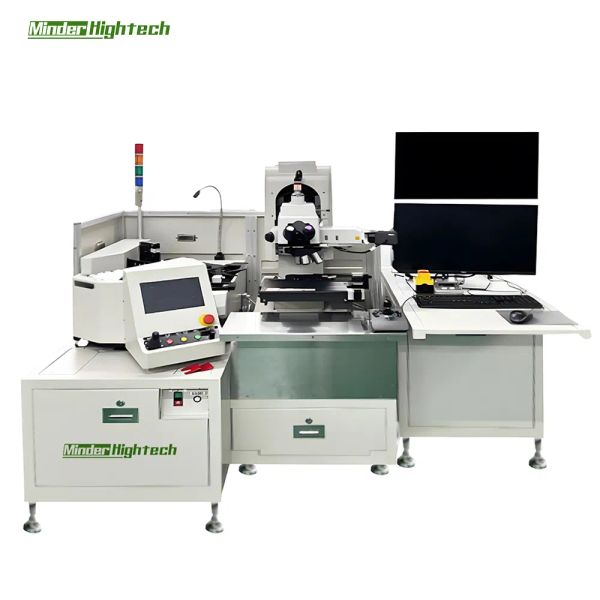
Semiconductor Wafer Re Evaluation Sampling Measurement Test Detecter Fully Automatic Ai Microscopic$230000
Seeopto Co., Ltd.
🇨🇳 China
20225-10 peopleManufacturer/Trading CompanyOEM manufacturer
ODM manufacturer
Product customization
Multinational enterprise
Key market
North America
Description
Seeopto Co., Ltd., established in 2022 and headquartered in the Pidu District of Chengdu, China, is a specialized manufacturer and trading company focused on precision-engineered optical solutions and advanced photonics materials. The company provides end-to-end services, including custom optics design, OEM manufacturing, and professional coating services. Its core expertise lies in the production of laser-grade crystals, including YAG-based (Nd:YAG, Er:YAG, Ho:YAG), YLF-based, and YVO4-based materials, as well as nonlinear optical (NLO) crystals such as KTP, LBO, and BBO.
Operating with a dedicated production line and R&D capabilities, Seeopto offers a comprehensive portfolio of optical components, including aspheric lenses, diffractive optical elements (DOE), micro lens arrays (MLA), waveplates, and polarizers. The company also specializes in semiconductor materials like Indium Phosphide (InP) and infrared optics utilizing silicon and germanium. Their advanced coating capabilities include anti-reflective (AR), high-reflecting, and polarization beamsplitter coatings, as well as various metal coatings (Au, Si, Al, Ti) designed for high damage thresholds.
Seeopto serves a diverse range of global industries, including aerospace, military, medical instrumentation, optical communication, and scientific research. With an established export license and a focus on high-quality composite materials and structural geometries, the company supports international clients with technical consulting and custom design submissions to meet complex system requirements.
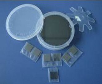
Inp (Indium Phosphide) Semiconductor/Substrate Material Light InP INgot or InP wafer$50
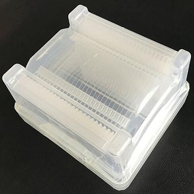
Glass Wafer Borofloat® 33 Lighting/Optics/Medical/Biotechnology/Semiconductor/Safety/Photovoltaic$50
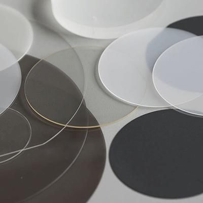
Fused Silica Optics/Semiconductor/Fiber/Solar Panels$50
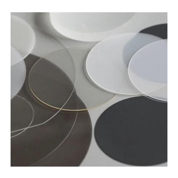
Fused Silica Optics Semiconductor Fiber Solar Panels$50
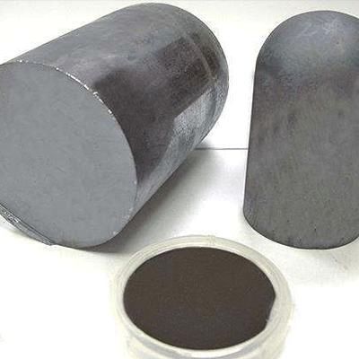
Inp (Indium Phosphide) Semiconductor/Substrate Material Light Source/Detector/Optical Fiber Communication$50
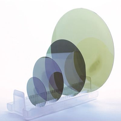
Sic (Silicon Carbide) LED Module Semiconductor Lighting Ingot-Chip-Epitaxial-Chip-Device-Module$50
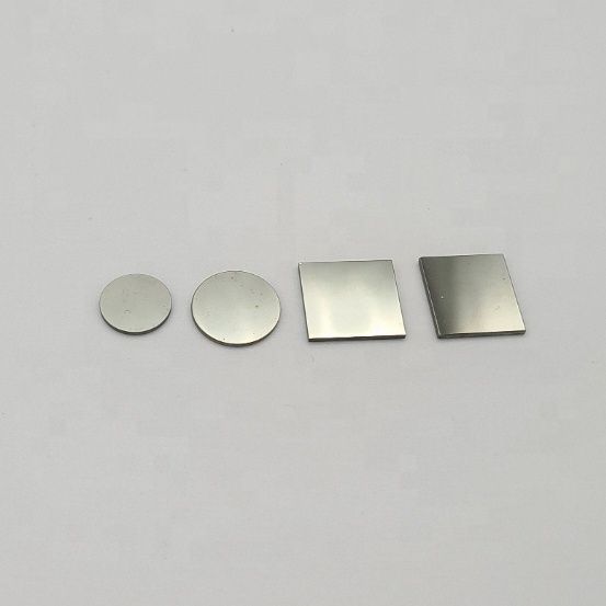
Single Crystal Silicon Ingot Fzn/CZ Purity 99.999999% Solar Cell/Semiconductor Integrated Circuit Silicon$200
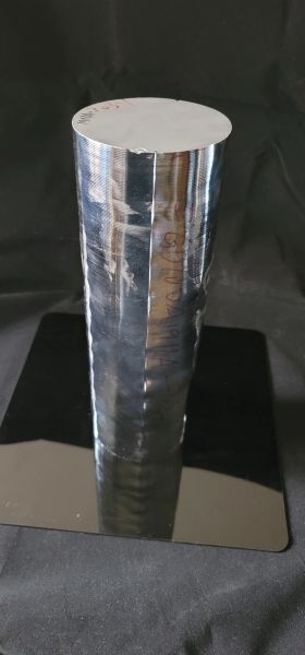
Single Crystal Silicon Ingot Fzn/CZ Purity 99.999999% Solar Cell/Semiconductor Integrated Circuit Silicon$200
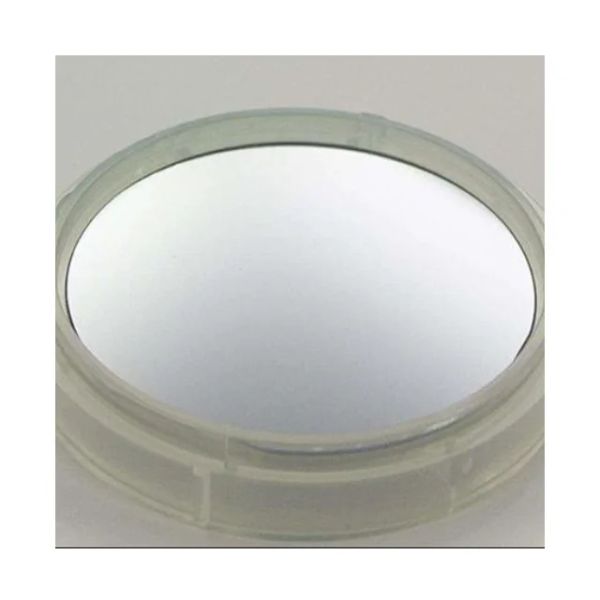
Gallium Arsenide (GaAs) LED Module for Semiconductor Lighting IR LED & Microwave Gunn Varsitydiode Optoelectronics$50
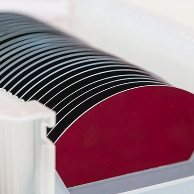
Fz Wafer up To10KΩ – Cm Dia 200mm Detectors\Solar$50
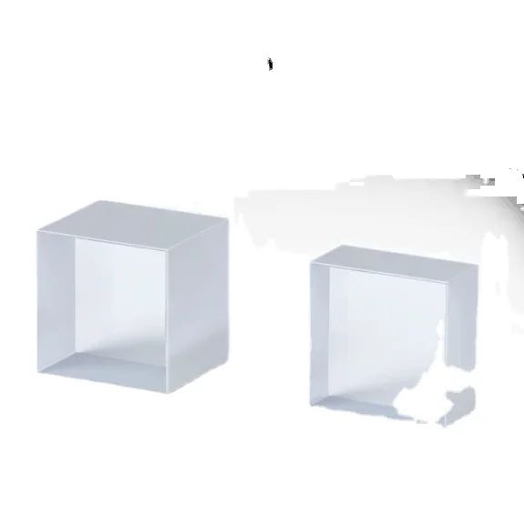
Lif Crystal Lithium Fluoride Fluoride Wafer for Substrate Application$150
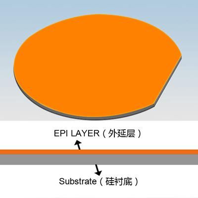
Epi Wafer Diodes/Transistors/Bipolar Ics/Eeprom/Amplifiers/RFID Epitaxy$50

Hunan Yujing Machinery Co., Ltd.
🇨🇳 China
19981001-2000 peopleManufacturerHigh capacity factory
Established brand
Large enterprise group
High-tech enterprise
Key customer
JA SOLAR
Key market
🇻🇳 Vietnam
Description
Hunan Yujing Machinery Co., Ltd. is a publicly listed smart equipment manufacturer (SZSE: 002943) established in 1998 and headquartered in Yiyang, China. Operating a 71,850 sqm facility with a workforce of approximately 2,000 employees, the company is a recognized Hi-tech Enterprise and a key participant in China's National Torch Project. It specializes in the research, development, and production of precision CNC machine tools and intelligent equipment designed for processing hard and brittle materials.
The company's comprehensive product portfolio includes multi-wire cutting machines, single-sided and double-sided grinding and polishing machines, diamond wire, and carbon/carbon composite materials. These solutions are critical for the precision processing of silicon wafers, sapphire, silicon carbide, magnetic materials, and ceramics. Beyond equipment manufacturing, the company provides one-stop silicon wafer cutting services and substrate conditioning equipment, serving high-growth sectors such as photovoltaics, semiconductors, consumer electronics, and new energy vehicles.
As an ISO 9001 and ISO 14001 certified manufacturer, Hunan Yujing Machinery offers OEM services and maintains a strong R&D focus, collaborating with research institutions to advance technologies in gallium oxide processing and ultra-precision surface finishing. The company serves a prestigious global clientele, including Foxconn, BYD, Epson, and NDK. While primarily focused on the domestic Chinese market, it maintains an active international presence, exporting its advanced machinery to the United States, Germany, Japan, Korea, and Southeast Asia.
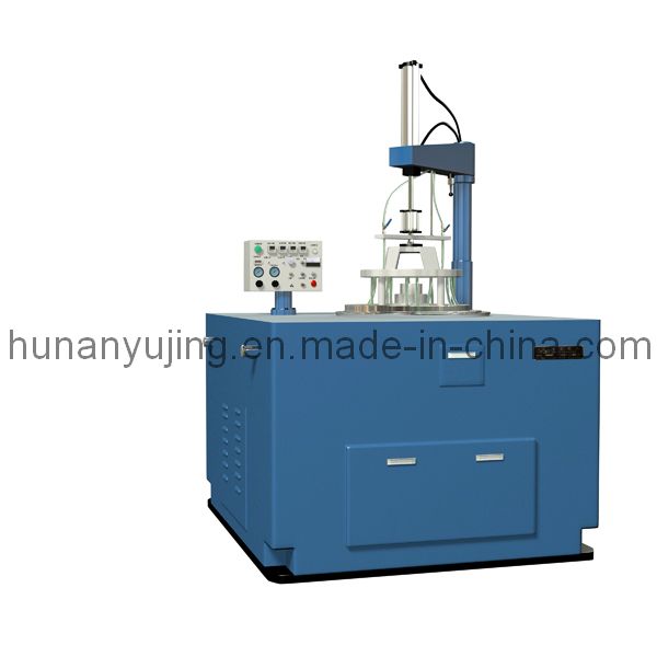
Semiconductor Lapping /Polishing Machine (YJ2M9B-5L(II) / (III))$25000
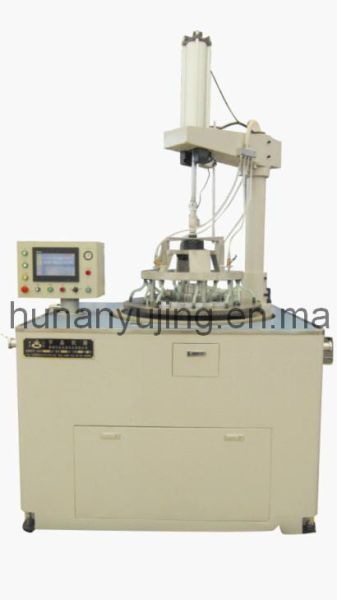
Ceramic Wafer Lapping /Polishing Machine (YJ2M13B-5L)$30000
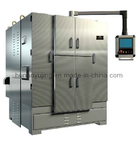
Diamond Multi-Wire Saw with Rocking Unit (YJXQ150(YB)) A$300000
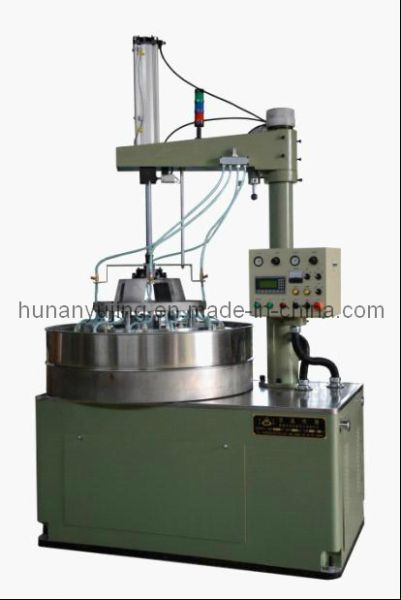
Optical Crystal Lapping Polishing Machine (YJ2M(P)13B-6L-A)$25000
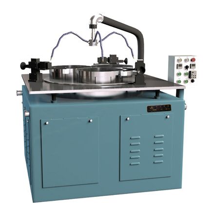
Ock-Typed Materials Side Lapping/Polishing Machine (YJDM950A)$10000
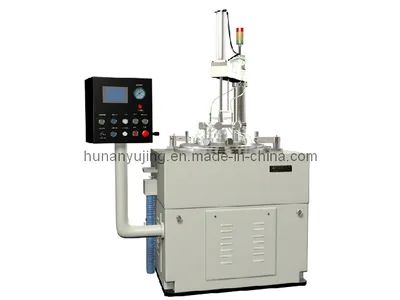
Optical Crystal Lapping Machine (YJ2M9.6B-10L(VII))
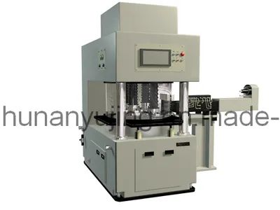
Single Side Pressurized Polishing Machine (YJDP910A)
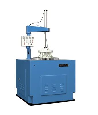
Optical Crystal Lapping /Polishing Machine (YJJP9.6S-5L)
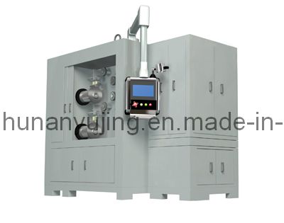
Amonocrystalline Silicon Cutting Machine (YJXQL1210B)$110000
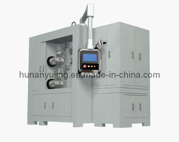
Crystal Wire Cutting Machine (YJXQL1416A)$100000
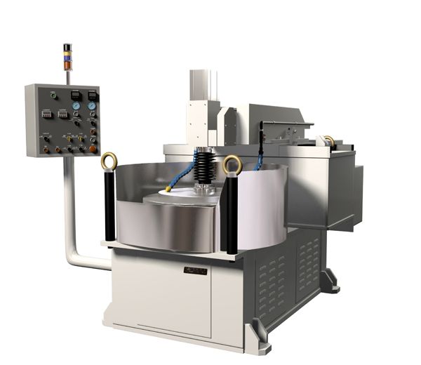
CSTN-LCD Single Side Polishing Machine (YJJP1200)$45000
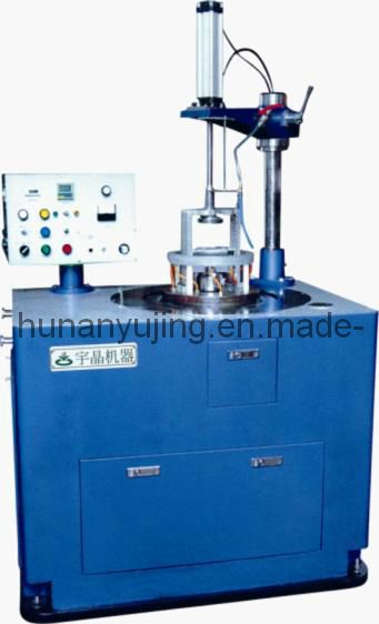
Crystal Quartz Polishing Machine (YJ2M6B-5L)$10000
How many suppliers does SourceReady track globally?
SourceReady tracks 4.0M+ suppliers globally across 200 sourcing countries and 7,000+ product categories.

Changsha Advanced Engineering Materials Limited
🇨🇳 China
201451-100 peopleManufacturer/Trading CompanyOEM manufacturer
ODM manufacturer
Product customization
High-tech enterprise
Key customer
GLOBAL SCIENTIFIC TECHNOLOGIES
Key market
🇧🇷 Brazil
Review
4.8
Description
Changsha Advanced Engineering Materials Limited, also known as Changsha Xinkang Advanced Materials Co., Ltd (Xinkang), is a premier high-tech manufacturer and trading company established in 2014. Based in Changsha, China, the company operates a 3,900㌑ facility and specializes in the R&D, production, and global distribution of advanced materials for PVD coating, aerospace, semiconductor, and renewable energy industries. With a workforce of approximately 50 to 100 trained professionals, the company provides one-stop solutions ranging from material design to high-efficiency mass production.
The company's extensive product portfolio includes over 1,000 items, featuring high-purity sputtering targets (metal, alloy, and ceramic), evaporation materials, and refractory metals such as Tungsten, Molybdenum, Tantalum, and Niobium. They are a specialized supplier of rare earth metals, oxides, and high-purity compounds, as well as ceramic materials like Silicon Carbide and Gallium Nitride wafers. Their manufacturing capabilities are supported by advanced equipment, including vacuum induction melting furnaces, sintering furnaces, and precision CNC machining for customized shapes such as rods, plates, foils, and wires.
Changsha Advanced Engineering Materials Limited maintains rigorous quality standards, holding ISO 9001, ISO 14001, and IATF 16949 certifications. The company serves a diverse international clientele, including research institutes and high-tech enterprises across North America, Europe, and East Asia. In addition to material supply, they offer technical services such as indium bonding, elastomer bonding, and material performance testing through an independent laboratory, ensuring high-performance solutions for flat panel displays, solar photovoltaics, and micro-electronics applications.
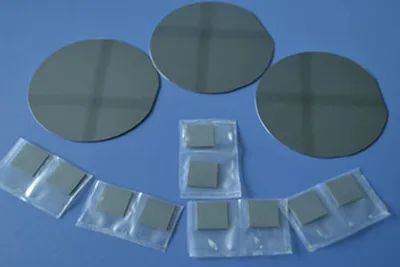
Semiconductor Gallium Arsenide Wafer (GaAs Wafer)
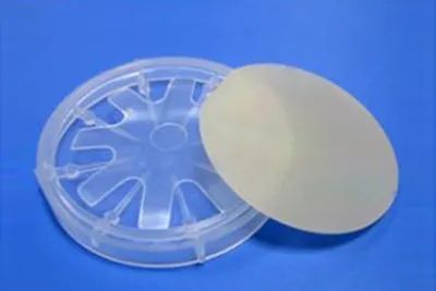
Gallium Nitride Wafer (GaN Wafer)

Silicon Carbide Wafer (SiC Wafer)
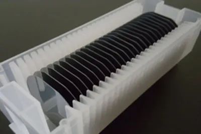
Gallium Antimonide Wafer (GaSb Wafer)
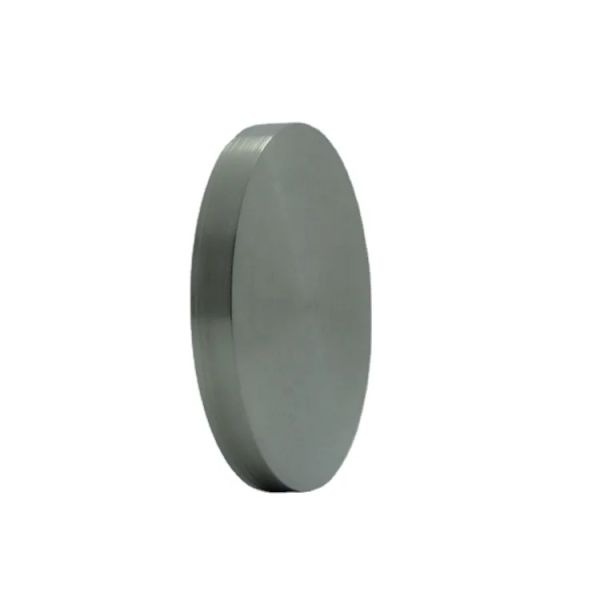
99.95% Pure Cobalt Sputtering target for Semiconductors Application$1852.12
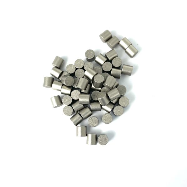
High Purity 99.995% Nickel Pellets for Semiconductor Industry$210
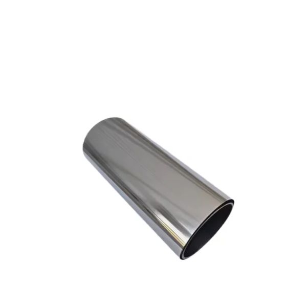
High Purity Tantalum Foil for Electronics and Semiconductors$2262663
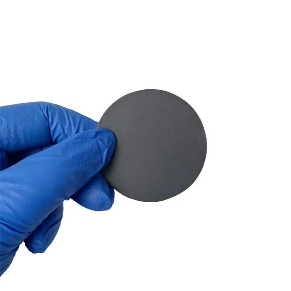
High Purity Boron Sputtering Targets for Semiconductor & Solar Applications$9260.58
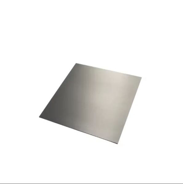
High Purity 99.99% Tantalum Sputtering Target for Semiconductor & Optical Coating$4723.5
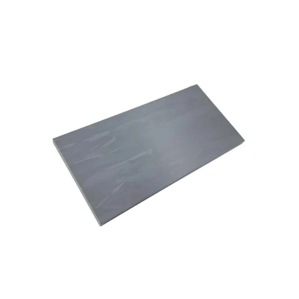
5N 6N Monocrystalline Silicon Target Silicon Sputtering Target for Semiconductor$45
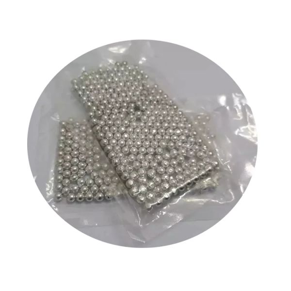
99.995% Indium Ball 1-10mm Metal Indium Pellets for Semiconductor Industry$55
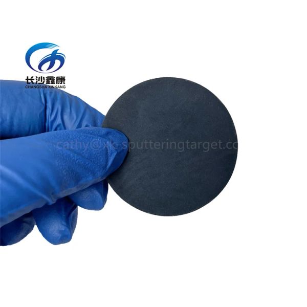
99.9% SmB6 Targets Rare Earth Samarium Hexaboride Sputtering Targets for Semiconductor$120

Qinhuangdao Intrinsic Crystal Technology Co., Ltd.
🇨🇳 China
2008301-500 peopleManufacturer/Trading Company/Wholesaler/Service CompanyOEM manufacturer
Product customization
Patented technology
High-tech enterprise
Key customer
TUBITAK
Key market
🇷🇺 Russia
Description
Qinhuangdao Intrinsic Crystal Technology Co., Ltd. is a high-tech manufacturer and service provider established in 2008, specializing in high-performance optical solutions across the infrared (IR) and ultraviolet (UV) spectrums. Based in Qinhuangdao, China, the company operates a 25,000-square-meter non-dust facility and employs between 300 and 500 professionals, including a specialized R&D team with 19 Ph.D. engineers. The company is recognized as China's largest fluoride supplier and a leading provider of silicon-germanium materials, with an annual output exceeding 80 tons of fluoride and 26 tons of silicon-germanium.
Intrinsic Crystal Technology integrates the entire industry chain, from crystal raw material growth to precision component fabrication and advanced optical coating. Their extensive product portfolio includes optical lenses (spherical, aspherical, plano-convex, and biconvex), windows, prisms, wafers, and beamsplitters. They work with a wide range of materials, including Calcium Fluoride (CaF2), Magnesium Fluoride (MgF2), Barium Fluoride (BaF2), Germanium (Ge), Silicon (Si), Zinc Selenide (ZnSe), and Zinc Sulfide (ZnS). These components serve critical applications in laser systems, gas analysis, thermal imaging, medical life sciences, defense, and semiconductor industries.
The company offers comprehensive OEM and ODM services, supported by 16 invention patents and modern CNC, diamond turning, and ZYGO testing equipment. Their manufacturing capabilities are backed by ISO 9001:2015, ISO 14001:2015, ISO 45001:2018, and RoHS certifications. With approximately 60% of its business dedicated to international trade, the company exports to over 60 countries and regions, including the USA, UK, Germany, Japan, and South Korea, serving global OEM customers and research institutions.
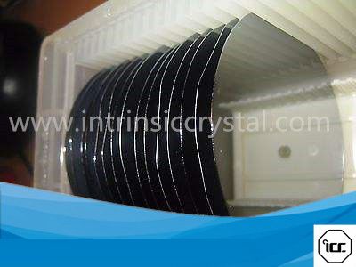
200mm Silicon Wafer for Power Semiconductor Devices$13
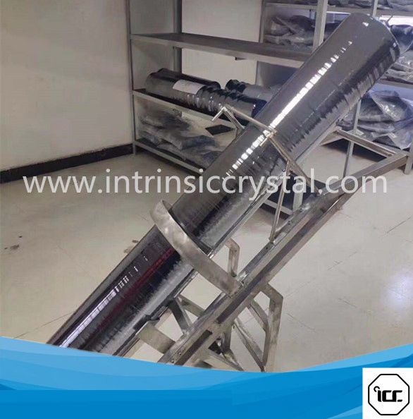
Semiconductor Silicon Wafer for N/P Type$13
Semi Silicon Wafer Manufacturer$13
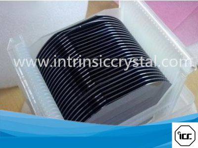
Optical Germanium B270 K9 Bk7 Silicon Quatz 1'~8" Wafer$20
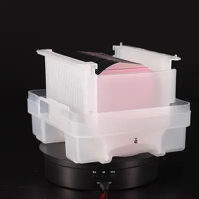
6 Inches*0.7mm/ 0.5mm Si Substrate/Double Side Polishing/Window Film/N/P/Single Crystal Silicon Wafer
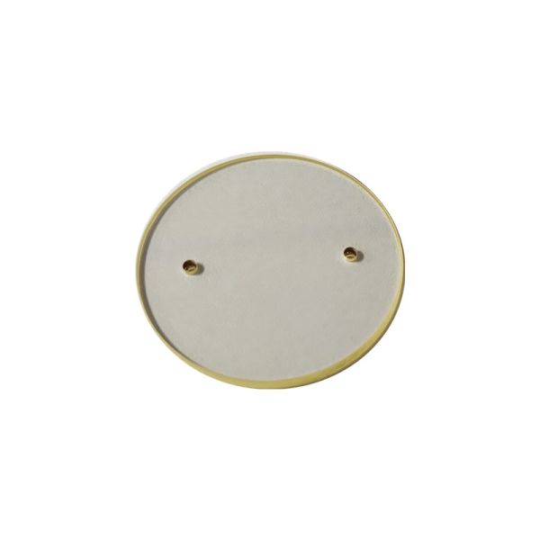
High Transmission/Low Absorption/Zinc Sulfide (ZnS) Round Opening Optical Window$10
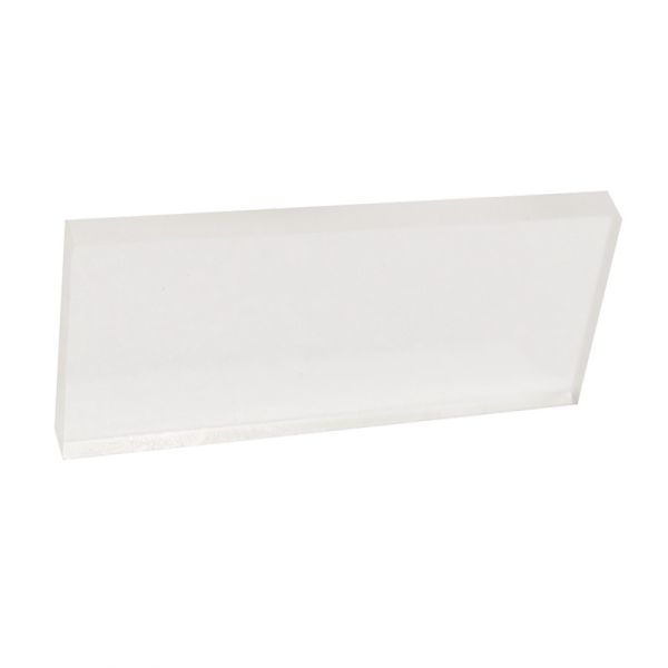
[Custom Processing] Bk7 Rectangular (Square) Optical Window [Factory Direct]$6
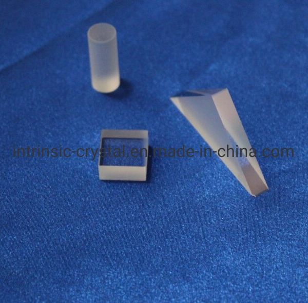
Right Angle Prisms, Optical Prisms$20
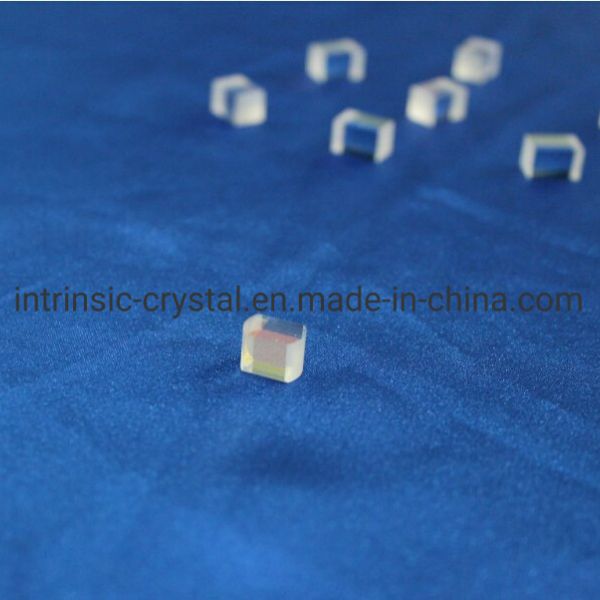
Porro Prisms, Optical H-K9 Glass Dove Prism$20
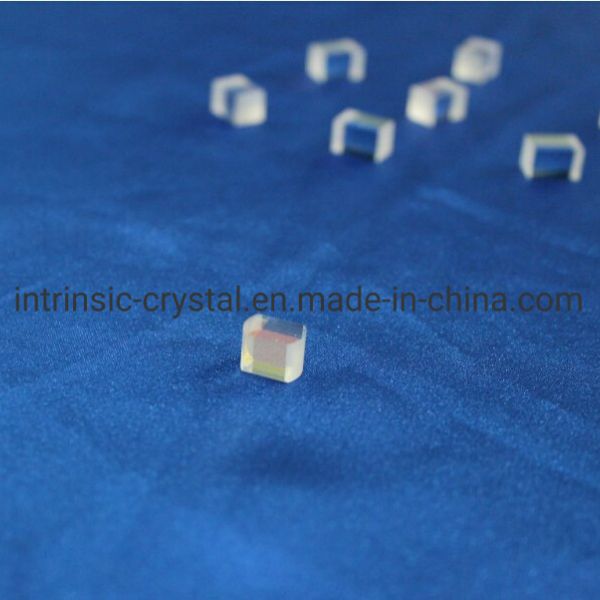
Polarizing Beam Splitting Cubes (High Power)$20
Germanium (Ge) Plano-Convex Lenses$25
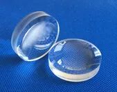
Precision Customized CaF2 Lenses From Intrinsic Crystal Technology-15 Years

Binzhou Aonuo New Material Technology Co., Ltd.
🇨🇳 China
20171001-2000 peopleManufacturerHigh capacity factory
Large enterprise group
Small batch production
Product customization
Key customer
FERROTEC
Key market
Asia
Description
Binzhou Aonuo New Material Technology Co., Ltd. is a manufacturer specializing in precision electronic ceramic substrates, established in 2017 with a registered capital of 30 million. The company operates with over 1000 employees and possesses advanced capabilities in new ceramic materials, powder preparation, molding technologies, and high-temperature sintering. They offer a comprehensive range of alumina-based products, including blank alumina substrates (96% and 99%), laser scribe alumina substrates, and unfired alumina tape. Their product portfolio also includes ceramic components, LED filaments, ceramic substrates for resistors, aluminum nitride substrates, and silicon nitride substrates. Binzhou Aonuo New Material Technology provides extensive customization options for alumina plates, covering dimensions, materials, surface finishes, and special features. The company is certified with ISO 9001:2015, IATF 16949, and ISO 14001, ensuring high-quality standards. Their products are engineered for superior thermal and electrical properties, serving high-power and high-frequency applications across diverse industries such as mobile phones, electronics, electrical engineering, communications, machinery, environmental protection, new energy, and biology. They offer OEM and ODM services and export their products globally.

Not Metallized Alumina Substrate for Semiconductor$0.04

Unfired Alumina Ceramic Plate for Semiconductor$0.04

Not Metallized Alumina Ceramic Sheet for Semiconductor$0.04
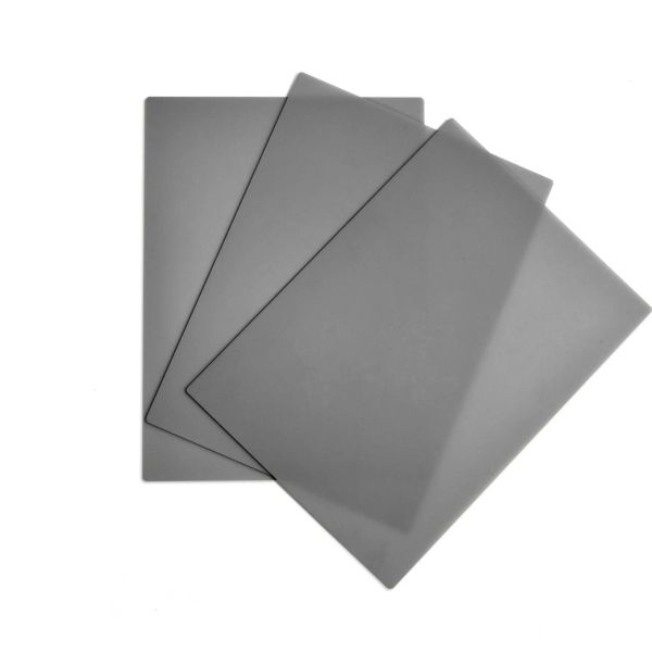
Insulating Substrate Si3n4 for Power Semiconductor Modules$17.65

Semiconductor Thin Film Aluminum Nitride Substrate Oxide for Circuit$3.68

Customized Semiconductor Thin Parts 96% 99% Laser Scribing Alumina Ceramics Substrate Manufacturer$0.04
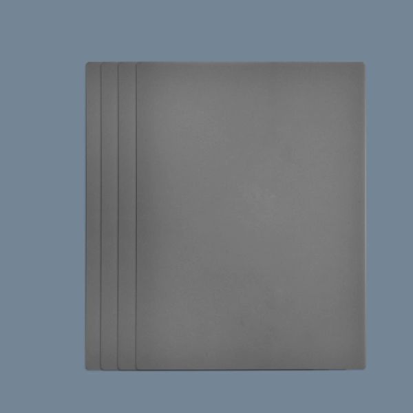
Robustness Silicon Nitride Wafer Manufacturer for Renewable Energy$17.65
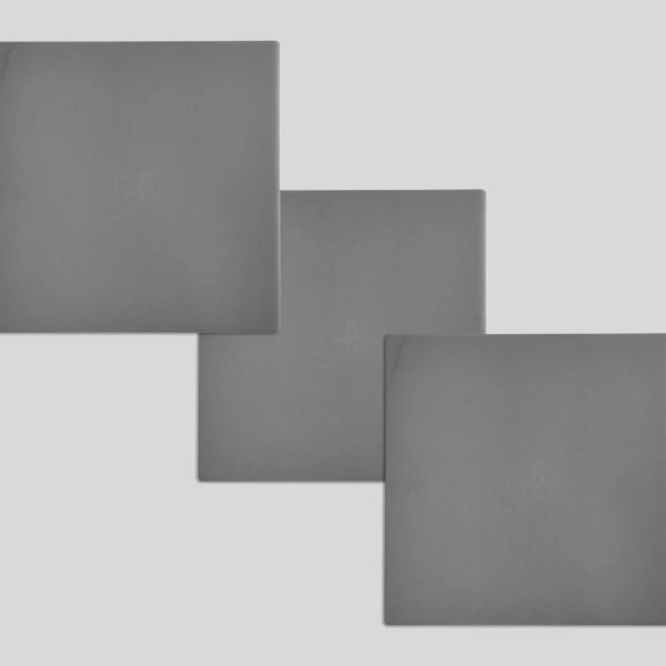
Tfc Thin Film Silicon Nitride Wafer in Microwave Circuits$17.65
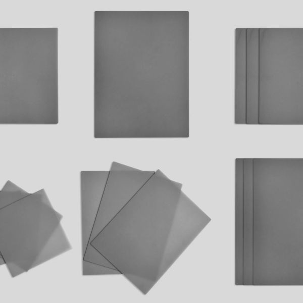
Tfc Thin Film Silicon Nitride Wafer in RF Modules$17.65
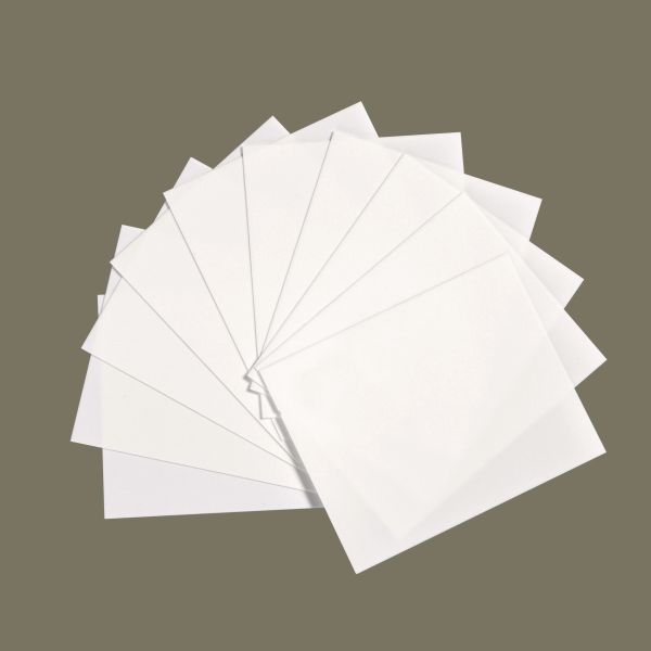
Thickness 1.5mm Alumina Ceramic Price Alumina Ceramic Wafer Carrier$0.04
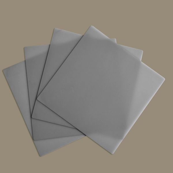
High Reliability Silicon Nitride Wafer Manufacturer for Renewable Energy$17.65
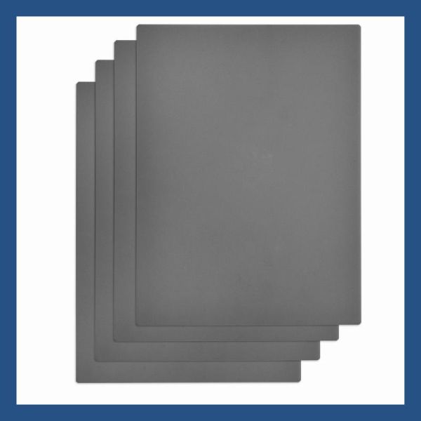
High Reliability Silicon Nitride Wafer Manufacturer for Automotive Power Electronics$17.65

Lianyungang Highborn Technology Co., Ltd.
🇨🇳 China
200811-50 peopleManufacturer/Trading CompanyProduct customization
Low MOQ
OEM manufacturer
ODM manufacturer
Key customer
IFARS
Key market
🇮🇳 India
Review
5
Description
Lianyungang Highborn Technology Co., Ltd., established in 2008 and based in Lianyungang, China, is a specialized manufacturer and trading company focused on high-performance quartz glass and precision ceramics. With over 15 years of industry experience, the company operates a factory equipped with eight production lines and approximately 50 machines, supporting a workforce of up to 50 employees. They are recognized for their expertise in fabrication technology and offer comprehensive OEM and ODM services, including custom design and sample processing supported by a dedicated R&D team.
The company’s extensive product portfolio is categorized into four primary areas: Precise Ceramics, Quartz Glass, Porous Ceramics, and Electric Apparatus. Their ceramic offerings include alumina, zirconia, silicon carbide, and silicon nitride components such as substrates, igniters, and industrial bushings. Their quartz glass division produces high-purity tubes, rods, plates, and laboratory glassware like cuvettes and crucibles. Additionally, they manufacture ozone generators, thick film resistors, and various porous ceramic filters and diffusers. These materials are engineered for high hardness, thermal shock resistance, and chemical stability, serving critical needs in the semiconductor, chemical, solar energy, textile, and laser industries.
Lianyungang Highborn Technology maintains a strong international presence, exporting to over 100 countries with a significant market share in North America and Europe. The company is committed to quality and safety standards, holding certifications including ISO 9001, CE, and RoHS, and complies with ASTM and FDA standards for specific product lines. Their reputation for reliability is further evidenced by a history of shipments to major international clients in the foodservice and laboratory sectors.
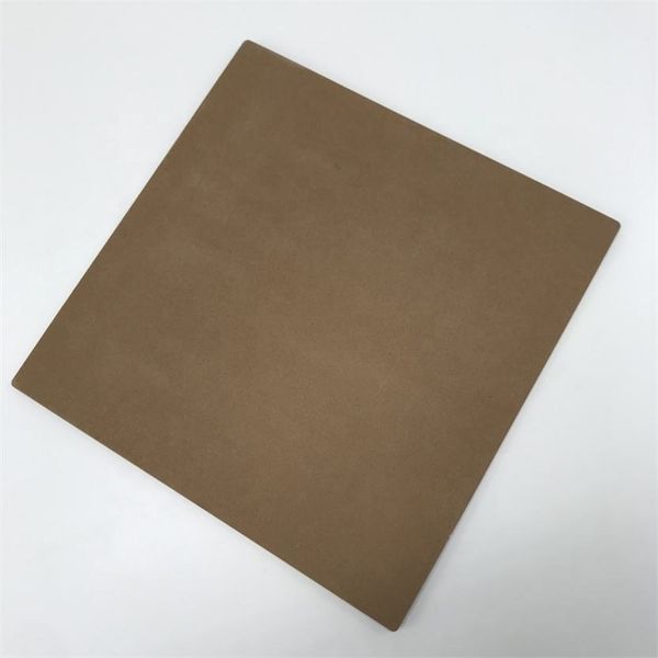
Microporous Ceramic Plate Silicon Carbide Ceramic Vacuum Sheet Semiconductor Wafer$20
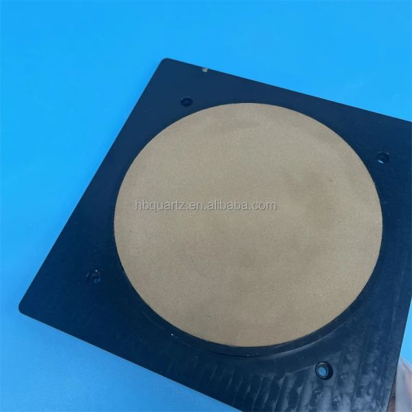
SSIC Silicon Carbide Wafer Microporous Ceramic Semiconductor Vacuum Chuck$715.23
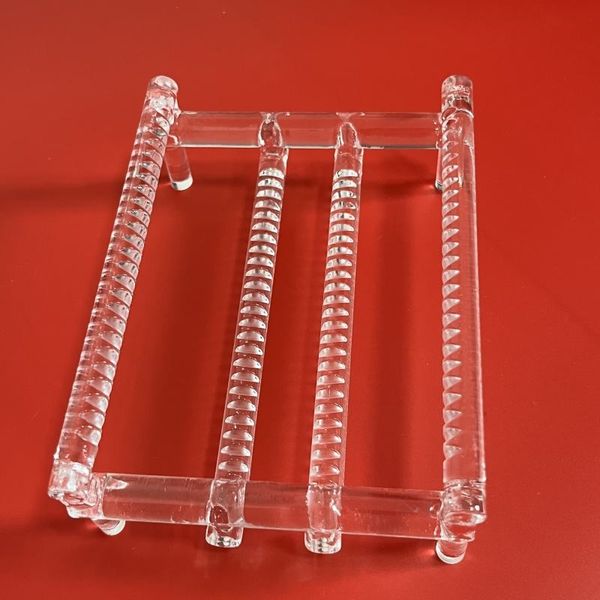
Semiconductor Manufacturing 99.99% High Purity Quartz Glass Wafer Carrier Boat$10
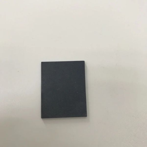
Porous Wafers Sucker Semiconductor Vacuum Adsorption Disc Microporous Ceramic Gas Disc$4423
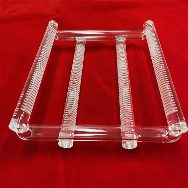
Customized Semiconductor Fused Quartz Silicon Wafer Carrier Optical Quartz Glass Boat$591.09
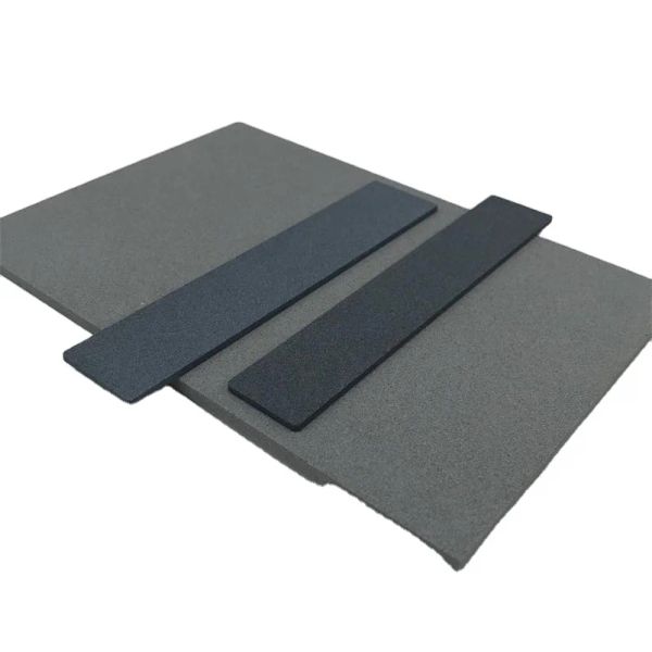
0.25-50 Um High Accuracy Factory Supply Semiconductor Porous Alumina Wafer Ceramic Vacuum Chuck Table$17732.7
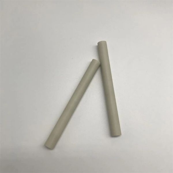
Semiconductor Aluminum Nitride Insulator ALN Ceramic Rod$450689
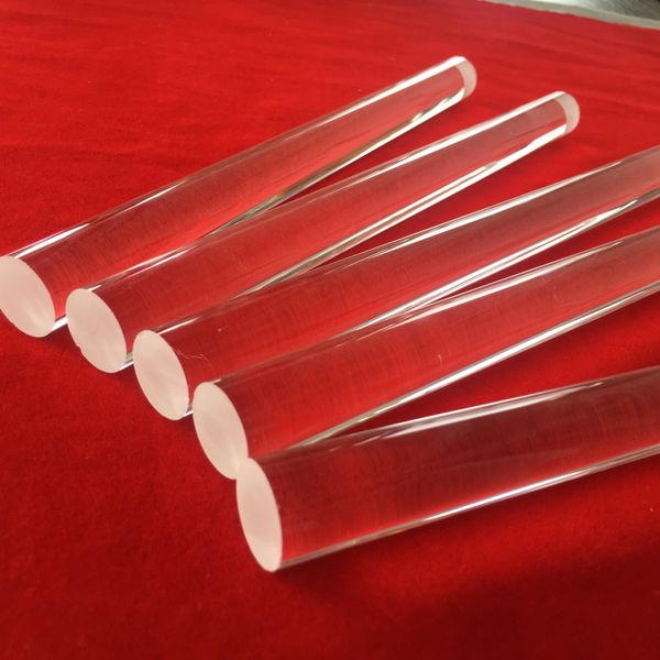
Corrosion Resistance Semiconductor clear Fused Silica Glass Cylinder Rod$10
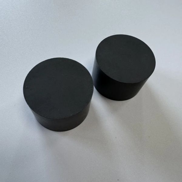
SiC Silicon Carbide Ceramic Block for Semiconductor Manufacturing Equipment$37558
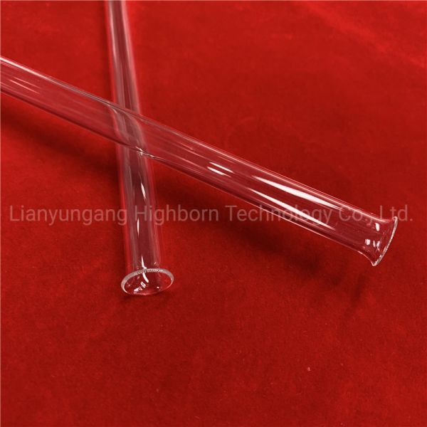
Two Ends Open Transparent Quartz Glass Pipe for Semiconductor$3
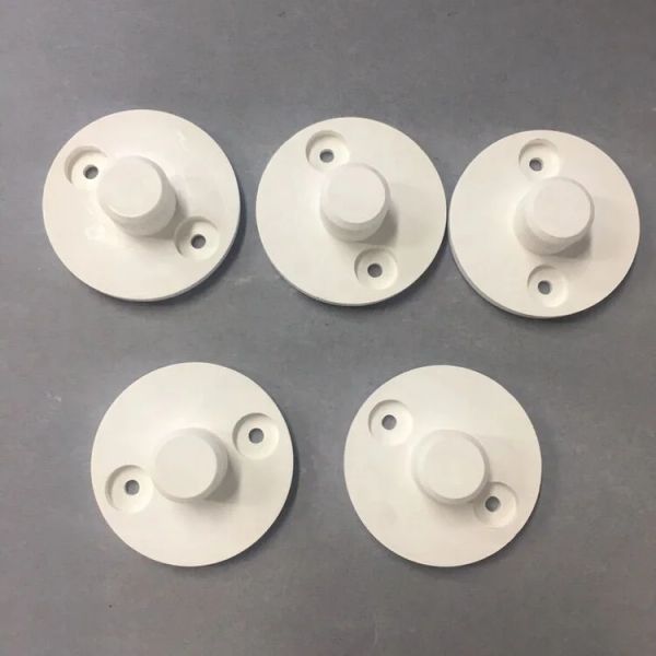
Semiconductor Field Machinable Parts Customized Boron Nitride Ceramic Structural Parts$686991
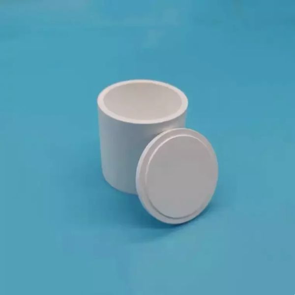
Customized PBN Boron Nitride VGF MBE OLE LEC Crucible for Semiconductor$9260.58

Trojan (Suzhou) Material Technology Co., Ltd.
🇨🇳 China
200551-100 peopleManufacturer/Trading Company/Service CompanyEstablished brand
OEM manufacturer
Own brand
Patented technology
Key customer
METKON
Key market
🇹🇷 Turkey
Review
3
Description
Trojan (Suzhou) Material Technology Co., Ltd. is a professional manufacturer and service provider specializing in metallographic testing equipment and consumables. Established in 2005 and headquartered in the Suzhou Industrial Park, China, the company has over 16 years of industry experience in material analysis and microstructure research. Operating from a 4,500 square meter production facility, Trojan provides comprehensive solutions for metallographic sample preparation, including cutting, mounting, grinding, polishing, and optical analysis.
The company's extensive product portfolio features independently developed high-end equipment such as the Alpha, Beta, and FlexPress series. Core offerings include automatic and manual cutting machines, hot and cold mounting presses, and high-precision grinding and polishing machines. They also supply a wide range of consumables, including abrasive cut-off wheels, diamond wafering blades, polishing cloths, and diamond suspensions. Furthermore, Trojan provides optical analysis instruments through partnerships with Leica and MN, alongside a full suite of hardness testers (Rockwell, Brinell, and Vickers).
Trojan serves a diverse range of industries, including PCB and SMT manufacturing, IC semiconductors, automotive, aerospace, and academic research institutions. As an ISO 9001 and ISO 14001 certified company, they maintain high quality and environmental standards, with many products also carrying CE and SGS certifications. With a professional R&D team and a robust technical sales network, the company supports over 1,000 customers globally. Trojan operates an international trade presence through its Hong Kong holdings, exporting to more than 50 countries across Europe, North America, and Southeast Asia.
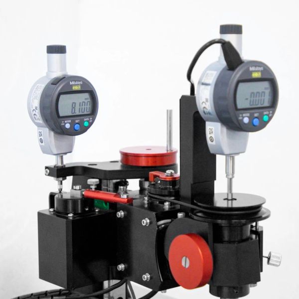
Precision Grinding Machine for Semiconductor$1050
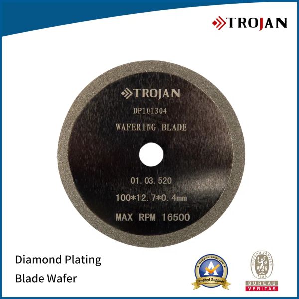
Diamond Plating Blade Sectioning Wafer Dp101304, Wafer Cutting Blade$1
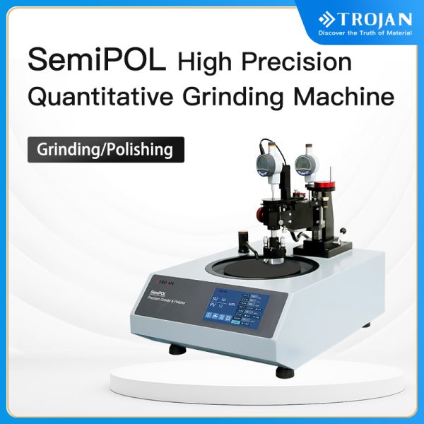
Semipol Lab High Precision Quantitative Metallographic Grinding Machine for Semiconductor$23470
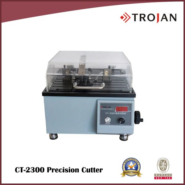
CT 2300 Precision Metallurgical Sample Cutting Machine for Cutting PCB SMT Semiconductor$2995
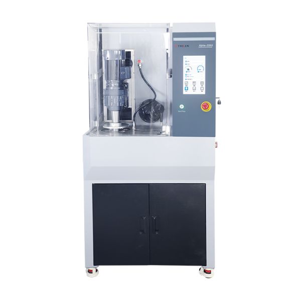
Alpha-335g Metallographic Slice Sand and Polish Semiconductor Chip Grinding and Polishing Machine Metallography Polishing$23470
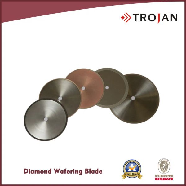
Wafering Blade for Cutting Hard Brittle Delicate Materials$30
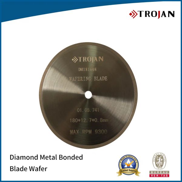
Dm Diamond Metal Bond Wafering Blade for Hard & Brittle Materials$100
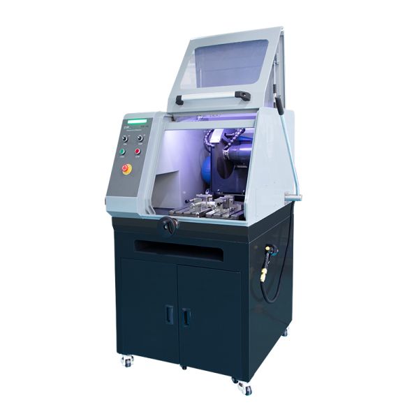
OEM/ODM CT-300 Lab-Use Metallographic Specimen Low Speed Cutting Equipment Laboratory Precision Rotation Metallographic Cutting Machine Semiconductor$7650
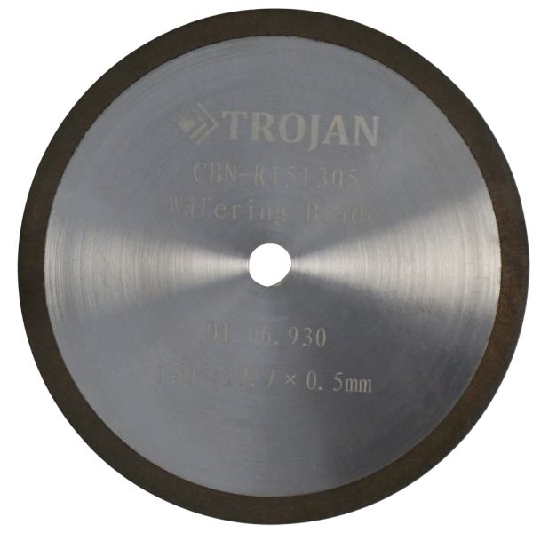
Metallographic Cutting Wafering Blades Metallographic Cutting Consumables Metallurgical Sample Cutting Specimen$77
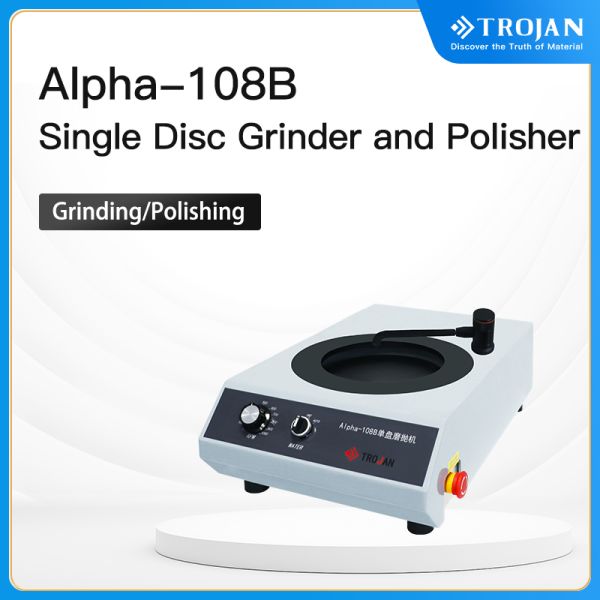
Alpha-108 Automatic Metallographic Sample Grinding Metallography Polishing Machine Wafer Polisher Grinder$1000
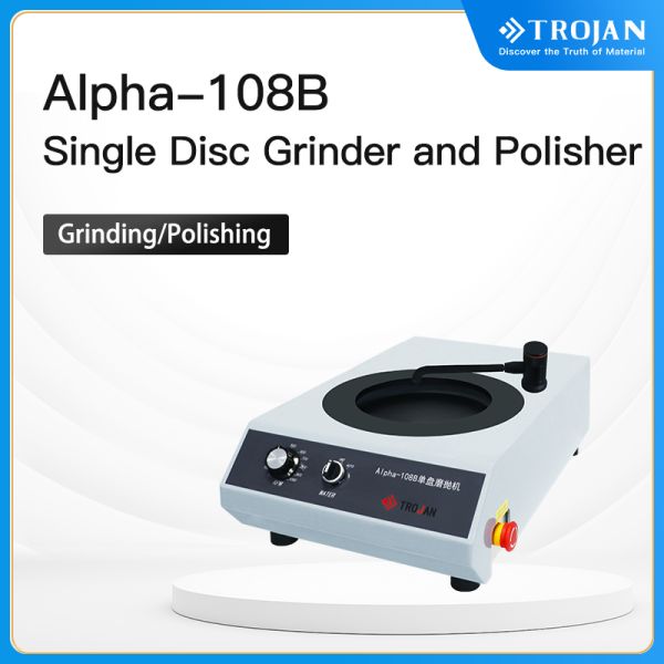
Alpha-108 Gold Phase Sample Grinding Machine Metallography Polishing Machine Wafer Polisher Grinder$1000
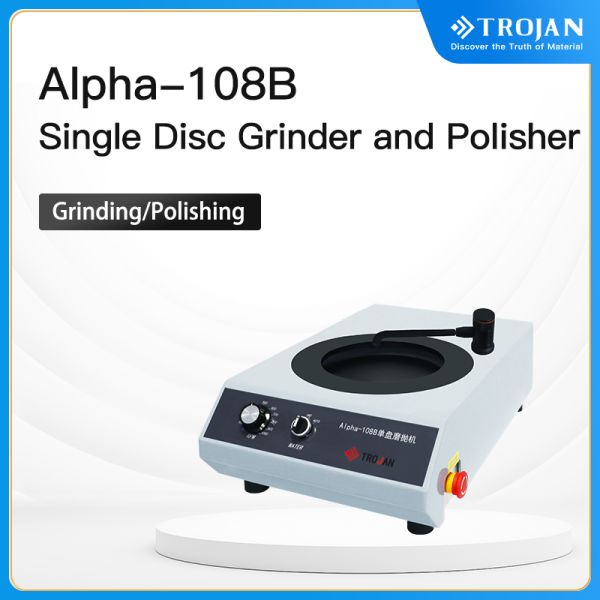
Alpha-108 Automatic Dual Platens Laboratory Tabletop Metallography Polishing Machine Metallography Wafer Polisher Grinder$1000

Hangzhou Dahe Thermo-Magnetics Co., Ltd.
🇨🇳 China
More than 10000 peopleManufacturer/Trading CompanyHigh capacity factory
Large enterprise group
OEM manufacturer
Multinational enterprise
Key customer
FERROTEC
Key market
🇲🇾 Malaysia
Description
Hangzhou Dahe Thermo-Magnetics Co., Ltd., a core subsidiary of the Ferrotec Group, is a large-scale international technology enterprise specializing in advanced materials and precision manufacturing. Based in Hangzhou, China, the company operates as both a manufacturer and trading entity with a workforce exceeding 10,000 employees. It holds a dominant market position in several high-tech sectors, ranking first in Asia for DCB ceramic substrate capacity and serving as the world's largest supplier of ferrofluidic vacuum feedthroughs. The company is also a global leader in the thermoelectric industry, maintaining a 40% international market share for thermoelectric modules.
With extensive manufacturing facilities and R&D centers, the company provides a comprehensive portfolio of semiconductor-related products, including 8-inch and 12-inch silicon wafers, precision quartz, ceramics, SiC parts, and quartz crucibles. Their technical capabilities extend to vacuum technologies, electron beam evaporators, and precision cleaning services for semiconductor components. As an OEM and ODM provider, they offer non-standard assembly services and metal processing for global industrial leaders such as Lam Research, Applied Materials, Samsung, and SK Hynix.
Hangzhou Dahe Thermo-Magnetics maintains rigorous quality standards, holding ASME certifications and domestic qualifications for pressure vessel manufacturing. The company demonstrates strong export capabilities with a significant trade history in North America, Europe, and Asia, supported by a complex global logistics network. Their diverse business units also produce industrial washing equipment, monocrystalline silicon ingots, and specialized cutting tools, catering to the automotive, medical, and photovoltaic industries.
FAQ
How can I compare multiple suppliers effectively?
Can I search for suppliers using one sentence?
Can enterprise teams use SourceReady for supplier research?